Semiconductor structure and manufacturing process thereof

a technology of semiconductors and manufacturing processes, applied in the direction of semiconductor devices, electrical equipment, basic electric elements, etc., to achieve the effect of enhancing breakdown voltage and reducing hot carrier

Active Publication Date: 2013-09-05
MACRONIX INT CO LTD
View PDF3 Cites 8 Cited by
  • Summary
  • Abstract
  • Description
  • Claims
  • Application Information

AI Technical Summary

Benefits of technology

[0005]The invention is directed to a semiconductor structure and a manufacturing process thereof, in which the thickness and the length of the dielectric layer are modulated to reduce the hot carrier effect and enhance the breakdown voltage.

Problems solved by technology

Therefore, it does not tend to design a MOS device having an off-state breakdown voltage toward to maximum.

Method used


Image

  • Semiconductor structure and manufacturing process thereof
  • Semiconductor structure and manufacturing process thereof
  • Semiconductor structure and manufacturing process thereof

Examples


Embodiment Construction

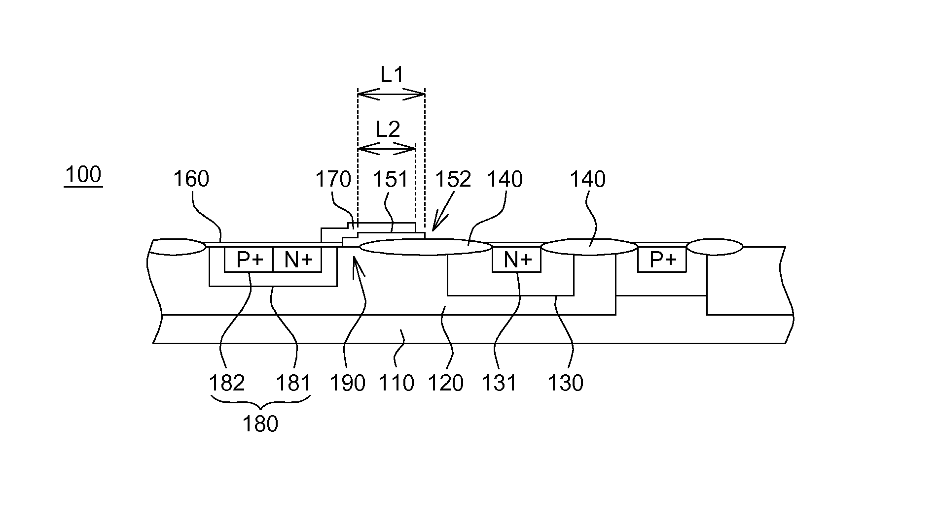
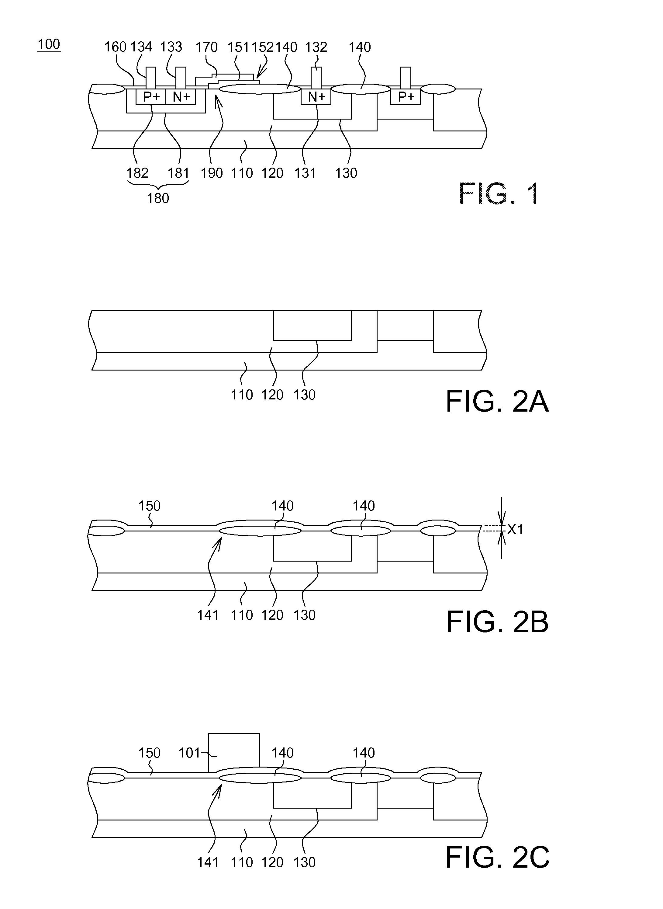
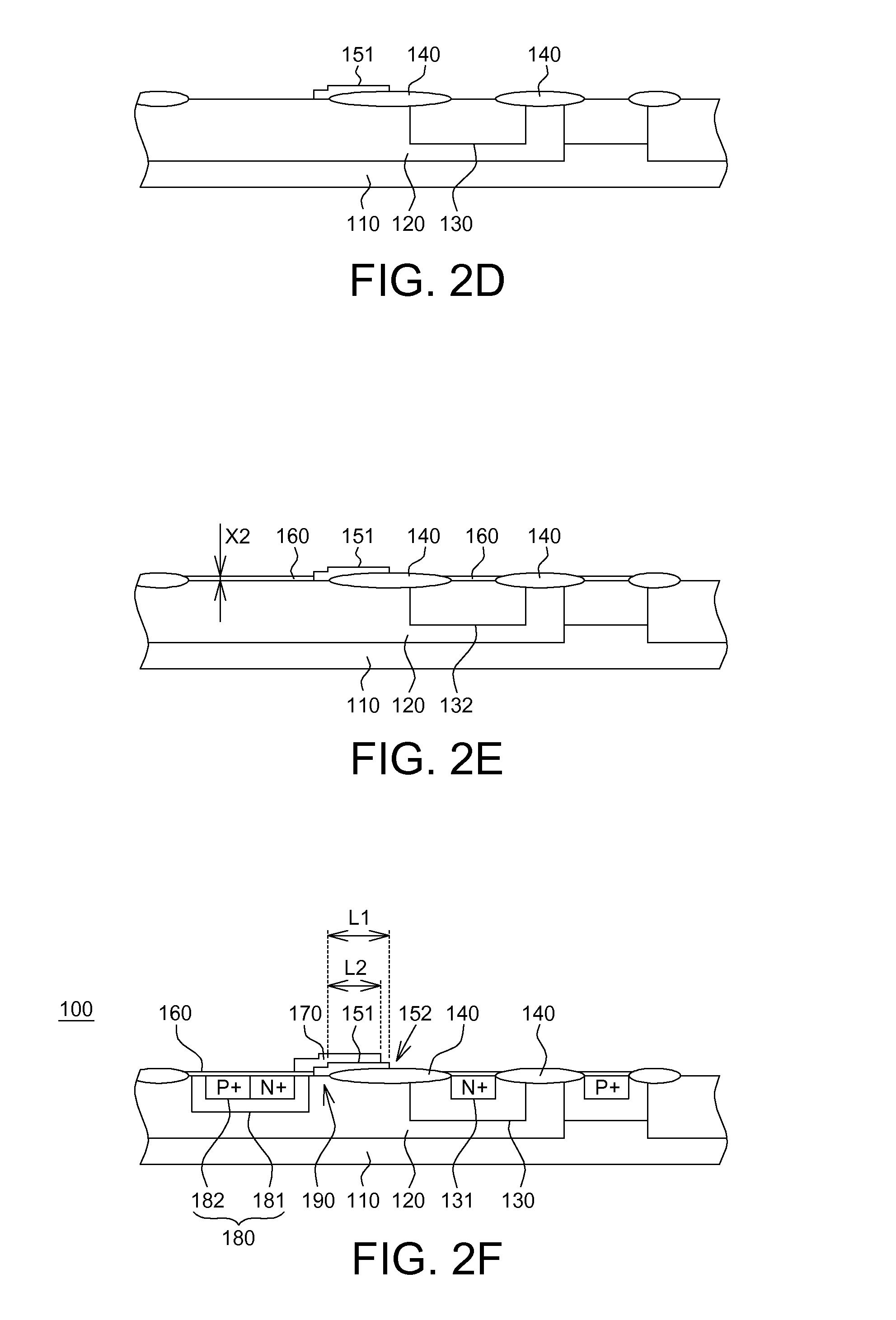
[0011]According to the semiconductor structure and the manufacturing process of the invention, the thick dielectric layer covered the edge portion of the field oxide, and the density of the tip electric field near the edge portion of the field oxide is lowered to reduce the hot carrier effect. In addition, with the isolation provided by two dielectric layers having different thickness, the breakdown phenomenon occurred between the gate conductive layer and the body can be prevented.

[0012]A number of embodiments are disclosed below for detailed descriptions of the invention only, not for limiting the scope of protection of the invention.

[0013]FIG. 1 is a schematic view illustrating a semiconductor structure according to an embodiment of the present invention. The semiconductor structure 100, such as a double diffusion metal oxide semiconductor device, includes a substrate 110, a well 120, a first doped region 130, a second doped region 180, a field oxide 140, a first dielectric layer...


PUM


Abstract

A semiconductor structure includes a substrate having a first conductive type, a well having a second conductive type formed in the substrate, a first doped region and a second doped region formed in the well, a field oxide, a first dielectric layer and a second dielectric layer. The field oxide is formed on a surface region of the well and between the first doped region and the second doped region. The first dielectric layer is formed on the surface region of the well and covers an edge portion of the field oxide. The first dielectric layer has a first thickness. The second dielectric layer is formed on the surface region of the well. The second dielectric layer has a second thickness smaller than the first thickness.

Description

BACKGROUND OF THE INVENTION[0001]1. Field of the Invention[0002]The invention relates in general to a semiconductor structure and a manufacturing process thereof, and more particularly to a metal oxide semiconductor (MOS) structure and a manufacturing process thereof.[0003]2. Description of the Related Art[0004]In the high voltage system, it is important for a metal oxide semiconductor (MOS) device having a high off-state breakdown voltage (Vbd) and a low on-state resistance (Ronsp), so that the MOS device can be operated under high voltage to allow a high current flowing between the drain and the source. Thus, the power consumption of the MOS device will be lowered. However, high off-state breakdown voltage and high on-state resistance generally come together, when the off-state breakdown voltage increases, the on-state resistance comparatively increases. Therefore, it does not tend to design a MOS device having an off-state breakdown voltage toward to maximum. It is an urgent prob...

Claims


Application Information

Patent Timeline
Patent Type & Authority Applications(United States)
IPC IPC(8): H01L29/772H01L21/336
CPCH01L29/401H01L29/42368H01L29/66681H01L29/66477H01L29/0878H01L29/1087H01L29/7816
Inventor CHIN, YU-HSIENHSU, CHIH-CHIAHUANG, YIN-FU
Owner MACRONIX INT CO LTD
Why Eureka
Try Eureka