Two-solder method for self-aligning solder bumps in semiconductor assembly

Inactive Publication Date: 2013-09-05
TEXAS INSTR INC
View PDF17 Cites 40 Cited by
  • Summary
  • Abstract
  • Description
  • Claims
  • Application Information

AI Technical Summary

Benefits of technology

[0009]Applicant solved the problem of reducing the viscous solder damping in a controlled range, when he discovered that precise self-alignment of solder joints in low-count and fine-pitch electrical bumps can be achieved by a practical and low-cost two-solder method: In addition to the electrically active function bumps, electrically inactive auxiliary alignment bumps are introduced (on the chip or on the substrate), which have a first solder alloy with a first eutectic temperature lower than the eutectic temperature of a second solder alloy applied for the electrically active function bumps.
[0010]After the auxiliary alignment bumps melt at the lower first eutectic temperature and collapse, they form auxiliary joints. While the temperature is raised to the higher eutectic temperature of the second alloy, the viscosity of these auxiliary joints, and thus the viscous damping, is lowered, allowing the auxilia

Problems solved by technology

Applicant saw that viscous damping results from friction of the molten solder and that this friction can be reduced by increasing

Method used


Image

  • Two-solder method for self-aligning solder bumps in semiconductor assembly
  • Two-solder method for self-aligning solder bumps in semiconductor assembly
  • Two-solder method for self-aligning solder bumps in semiconductor assembly

Examples


Example

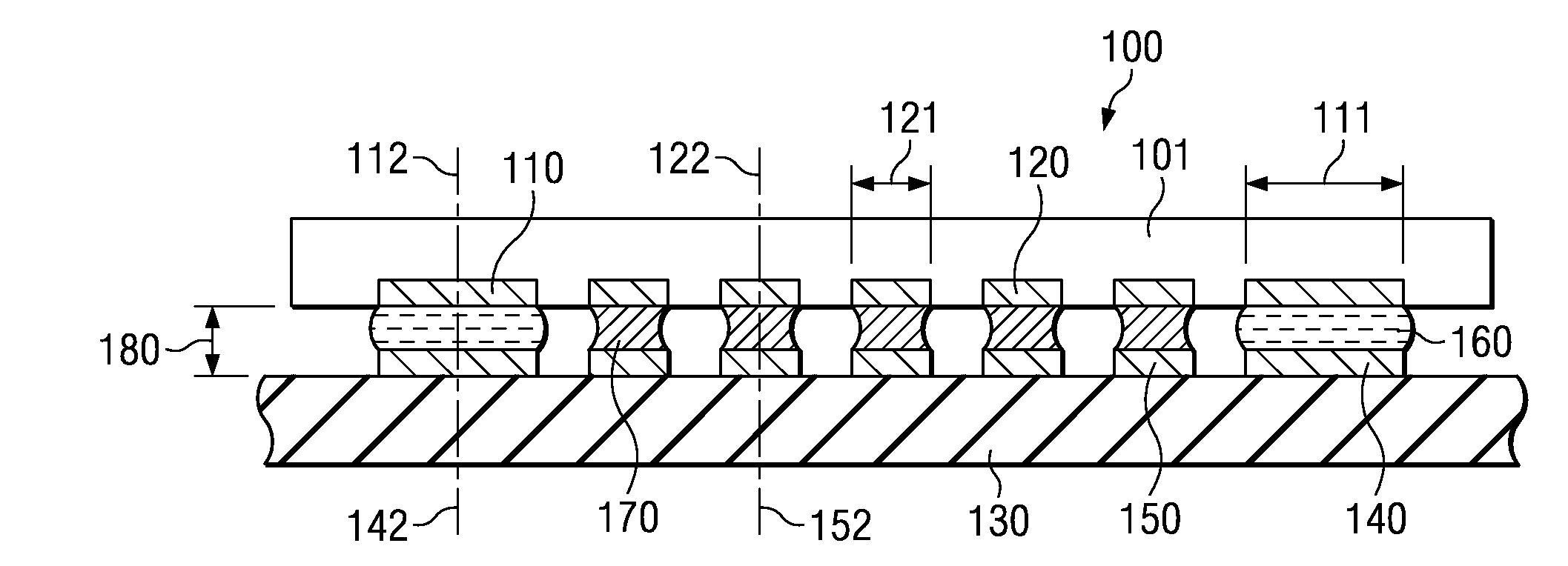
[0020]FIG. 1 illustrates an exemplary embodiment of an assembled device generally designated 100. Device 100 includes a semiconductor chip 101 with a first set of metallic contact pads 110 and a second set of metallic contact pads 120. The first contact pads 110 have a first area, indicated in FIG. 1 by linear dimension 111, and may be electrically inactive; pads 110 are herein referred to as alignment pads. Second contact pads 120 have a second area, indicated in FIG. 1 by linear dimension 121, and are electrically active; pads 120 are herein referred to as function pads. Preferably, the first area is greater than the second area, but in other embodiments they may be equal. The first and the second contact pads are made of a metal such as copper or aluminum and have a surface metallurgically configured to be wettable and solderable. As an example, the contact pad surfaces may include a layer of nickel followed by a layer of palladium and an outermost layer of gold.

[0021]Device 100 ...


PUM

PropertyMeasurementUnit
Melting pointaaaaaaaaaa

Abstract

A semiconductor device (100) comprising a semiconductor chip (101) assembled on a substrate (130) by solder joints; the chip and the substrate having a first set of contact pads (110, 140) of a first area, respective pads vertically aligned and connected by joints (160) made of a first solder having a first volume and a first melting temperature; and the chip and the substrate having a second set of contact pads (122, 150) of a second area, respective pads vertically aligned and connected by joints (170) made of a second solder having a second volume and a second melting temperature, the first melting temperature being lower than the second melting temperature.

Description

FIELD OF THE INVENTION[0001]The present invention is related in general to the field of semiconductor devices and processes, and more specifically to the structure and fabrication method self-aligning two-solder bumps in assembly of low bump-count fine-pitch semiconductor devices.DESCRIPTION OF RELATED ART[0002]Since IBM first introduced a soldering technology called Controlled Collapse Chip Connection (commonly known as C4) about four decades ago, many advantages of this technology have been realized: batch assembly, self-aligning capability, high interconnection density, high yield, and low cost. The self-alignment mechanism in particular is important for semiconductor devices with high bump count and fine bump pitch.[0003]In the solder self-alignment mechanism, the molten solder wets the metal pad and forms a solder joint; however, this joint may be misaligned. The restoring surface tension, a force acting on the unit length of the surface (Newton per meter, kg·s−2), is proportio...

Claims


Application Information

Patent Timeline
IPC IPC(8): H01L23/498B23K31/02
CPCH01L24/16H01L24/17H01L2224/81986H01L2224/81815H01L2224/81805H01L2224/8146H01L24/81H01L2224/0401H01L2224/81493H01L24/13H01L24/14H01L2224/05624H01L2224/05644H01L2224/05647H01L2224/0603H01L2224/13111H01L2224/1403H01L2224/14505H01L2224/14517H01L2224/16238H01L2224/16506H01L2224/81143H01L2224/81191H01L2224/81424H01L2224/81447H01L2924/00014H01L2924/01047H01L2924/01029H01L2924/01028H01L2924/00012H01L2924/01083H01L2924/01049H01L2924/01082H01L2924/0103H01L2924/01079H01L2224/17517H01L2924/01322H01L2924/00
Inventor MAWATARI, KAZUAKI
Owner TEXAS INSTR INC
Why Eureka
Try Eureka