Eureka AIR delivers breakthrough ideas for toughest innovation challenges, trusted by R&D personnel around the world.

Semiconductor device

Active Publication Date: 2013-09-19
MITSUBISHI ELECTRIC CORP
View PDF12 Cites 4 Cited by
  • Summary
  • Abstract
  • Description
  • Claims
  • Application Information

AI Technical Summary

Benefits of technology

The present invention improves both heat-dissipation and insulation performance by using two insulation layers with different characteristics on both sides of the metal base plate.

Problems solved by technology

However, electric field concentration by the inorganic filler in the proximity of the filler has not been taken into consideration, thereby raising a problem in that the insulation performance is deteriorated.
Moreover, when a ceramic substrate is used as in Patent document 1 etc., high withstand voltage is achieved by thickening the ceramic substrate; however there has been another problem in that the thickening of the ceramic substrate, which becomes an insulation layer, increases thermal resistance, thereby deteriorating the heat-dissipation performance.

Method used


Image

  • Semiconductor device
  • Semiconductor device
  • Semiconductor device

Examples


embodiment 1

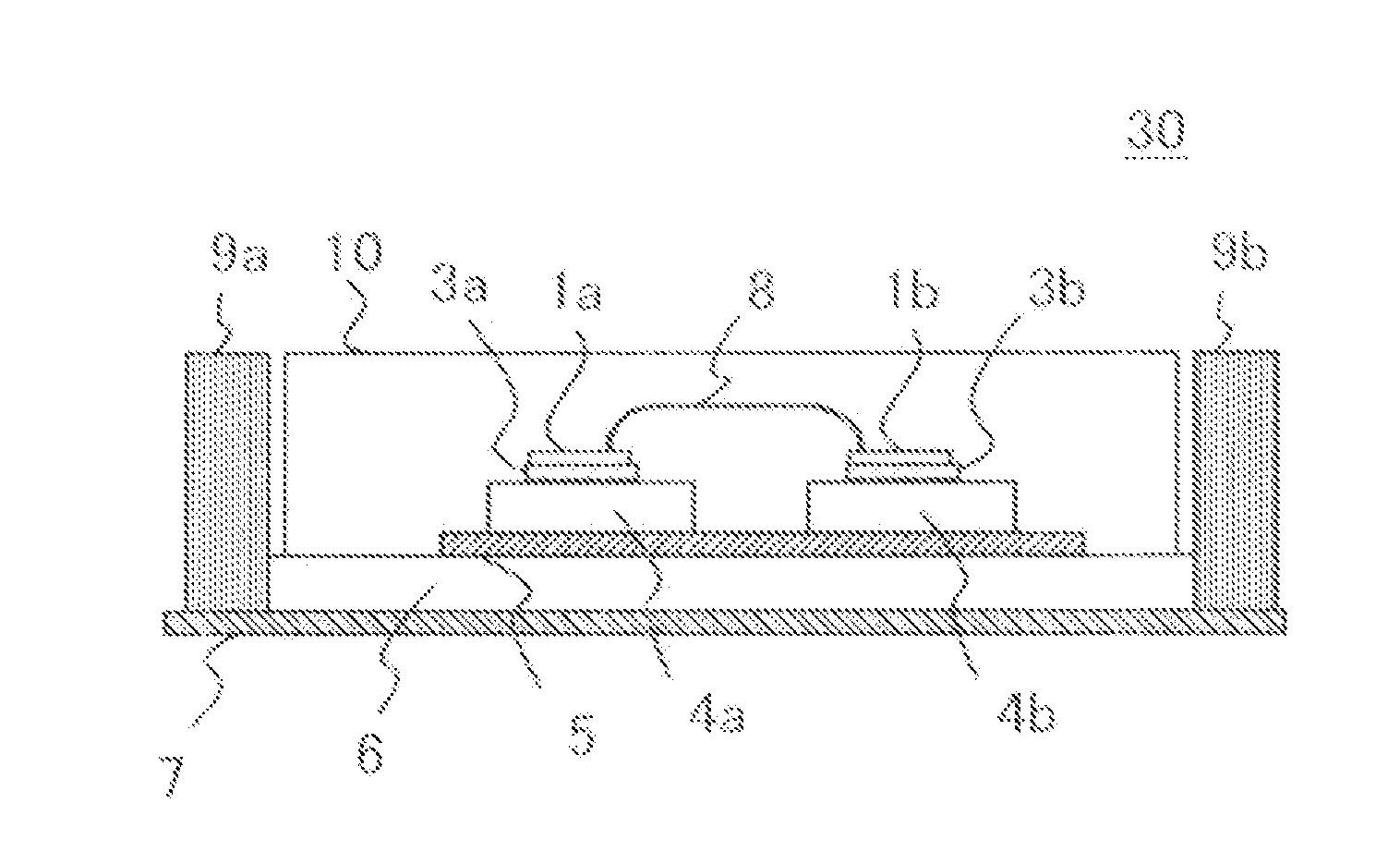
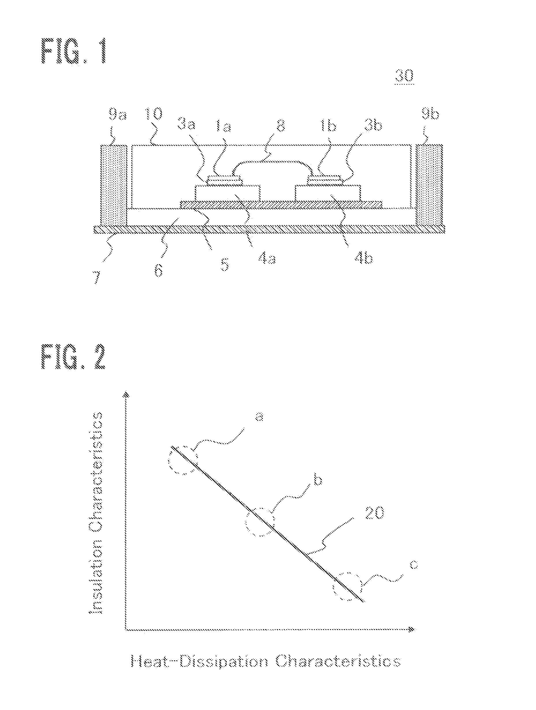
[0017]FIG. 1 is a cross-sectional view showing a semiconductor device according to Embodiment 1 of the present invention. The semiconductor device 30 shown in FIG. 1 is an example in which two semiconductor elements, 1a and 1b, are mounted. The semiconductor device 30 includes lead frames (conductive members) 4a and 4b on which the semiconductor elements 1a and 1b are mounted; cooling units 9a and 9b that dissipates heat generated by the semiconductor elements 1a and 1b; and a metal base plate 6 connected to the cooling units 9a and 9b. The semiconductor elements 1a and 1b are mounted on their respective lead frames 4a and 4b; the semiconductor element 1a is connected to the lead frame 4a and the semiconductor element 1b is connected to the lead frame 4b. The semiconductor elements 1a and 1b are soldered to the lead frames 4a and 4b with solder 3a and 3b, respectively. The semiconductor elements 1a and 1b are electrically connected with each other by a wire 8. Moreover, the semicond...


PUM


Abstract

A semiconductor device including: a semiconductor element; a lead frame connected to the semiconductor element; a metal base plate mounted on the lead frame via a first insulation layer; and a second insulation layer disposed on the opposite side of the metal base plate face on which the first insulation layer is disposed; wherein the first insulation layer is an insulation layer whose heat-dissipation performance is higher than that of the second insulation layer, and the second insulation layer is an insulation layer whose insulation performance is the same as that of the first insulation layer or higher than that of the first insulation layer.

Description

TECHNICAL FIELD[0001]The present invention relates to semiconductor devices mounted with semiconductor elements such as IGBTs and diodes.BACKGROUND ART[0002]Until now, a semiconductor device mounted with semiconductor elements that generate heat attributable to their operation includes a metal base plate made of metal such as copper that excels in thermal conductivity, in order to enhance heat-dissipation performance. In a conventional semiconductor device, heat generated by semiconductor elements is dissipated through an organic insulation sheet and ceramic substrate to a metal base plate connected to a cooling unit. In recent years, the heat-dissipation characteristics need to be enhanced even more with growing high-density integration of the semiconductor elements.[0003]A semiconductor device is disclosed in Patent document 1, in which a ceramic insulation substrate is disposed on a metal base plate via solder, and in addition on the ceramic insulation substrate are mounted semic...

Claims


Application Information

Patent Timeline
IPC IPC(8): H01L23/495H01L29/16
CPCH01L23/36H01L24/32H01L2924/1305H01L2224/32013H01L2224/48091H01L24/48H01L24/73H01L25/0655H01L25/072H01L2224/48137H01L2224/73265H01L2924/10253H01L2924/10272H01L2924/1033H01L2924/1203H01L2924/13055H01L2924/14H01L23/49568H01L29/1602H01L29/1608H01L23/3121H01L2224/32245H01L2924/00014H01L2924/00H01L2224/45099H01L2224/45015H01L2924/207
Inventor SHIOTA, HIROKIOKA, SEIJIYAMAGUCHI, YOSHIHIRO
Owner MITSUBISHI ELECTRIC CORP
Why Eureka
Eureka Blog
Learn More