Semiconductor light-emitting device and manufacturing method thereof

a technology of semiconductors and light-emitting devices, which is applied in the manufacture of semiconductor/solid-state devices, semiconductor devices, and electrical devices, etc., can solve the problems of reducing the light extraction efficiency of the light emitted by the light-emitting diode, affecting the uniformity of light emitted, and damage to the light-emitting diode or the light-emitting efficiency of the light-emitting diode, so as to achieve high light extraction efficiency

Inactive Publication Date: 2013-09-19
GENESIS PHOTONICS
View PDF5 Cites 5 Cited by
  • Summary
  • Abstract
  • Description
  • Claims
  • Application Information

AI Technical Summary

Benefits of technology

[0007]The invention provides a semiconductor light-emitting device and a manufacturing method thereof, and the semiconductor light-emitting device has a high light extraction efficiency.

Problems solved by technology

The current is over-concentrated in a small region between the two electrodes, which not only results in the non-uniformity of the light emitted, but is also easy to lead to the damages of the light-emitting diode or light-emitting efficiency decreased of the light-emitting diode out of poor heat dissipation because of the over-concentration of the heat generated through the flow of the current.
In addition, provided that the surface removed by etching in the vertical direction is a vertical surface, which easily results in the decreases of the light extraction efficiency of the light emitted by the light-emitting diode due to total reflection within the semiconductor light-emitting device.

Method used


Image

  • Semiconductor light-emitting device and manufacturing method thereof
  • Semiconductor light-emitting device and manufacturing method thereof
  • Semiconductor light-emitting device and manufacturing method thereof

Examples


Embodiment Construction

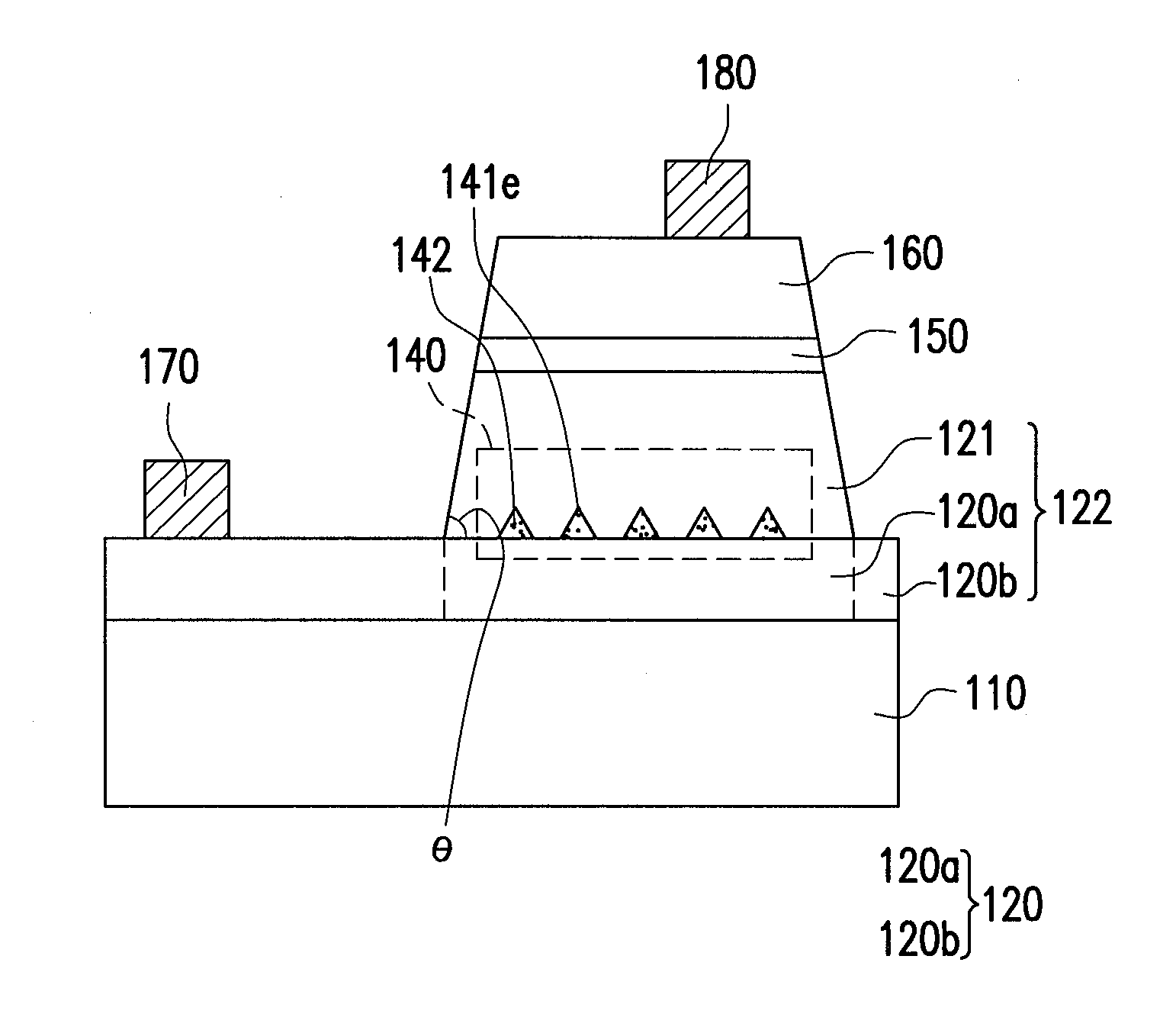
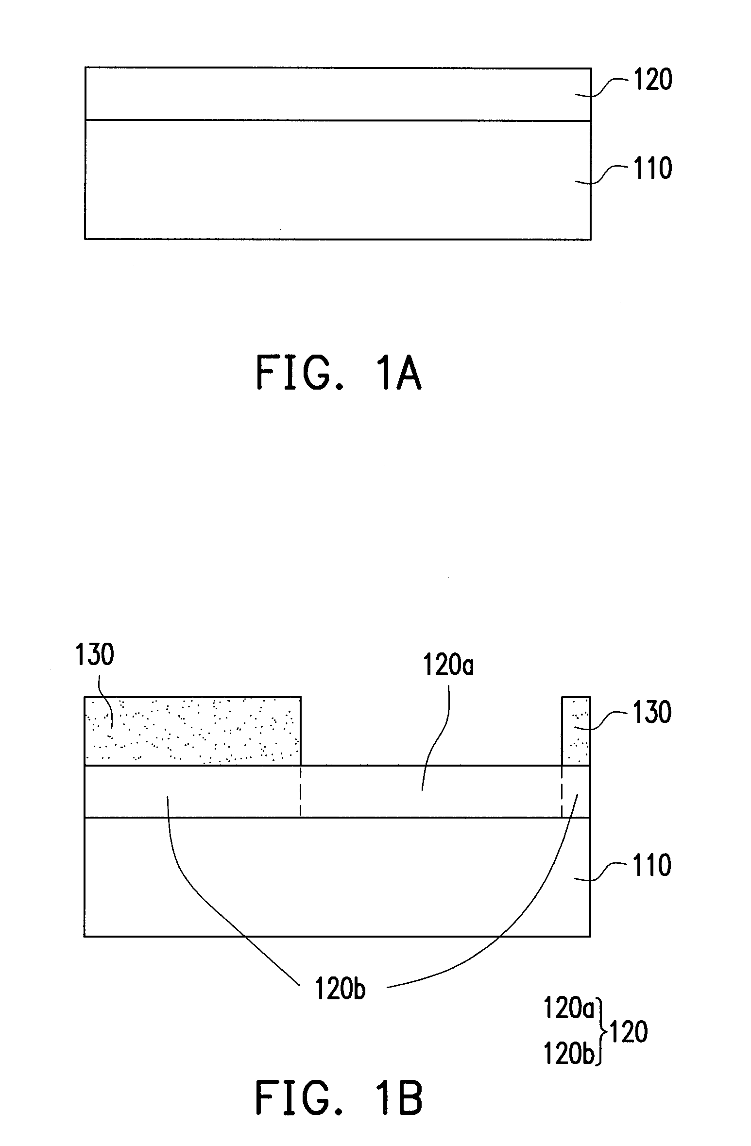
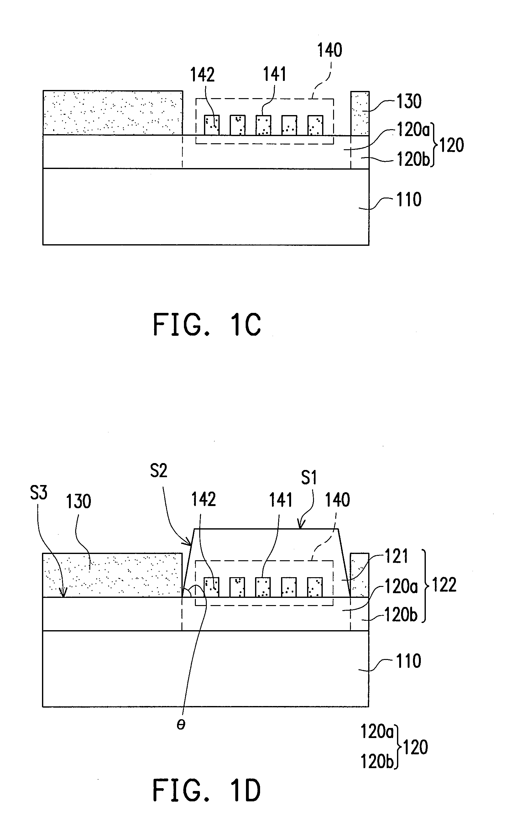
[0021]FIGS. 1A through 1F are schematic cross-sectional views illustrating a process flow of manufacturing a semiconductor light-emitting device according to one embodiment of the invention.

[0022]Please refer to FIG. 1A first. First, a first type doped semiconductor material is grown on a substrate 110 to form a base portion of a first type doped semiconductor 120, wherein the substrate 110 is, for example, a silicon substrate, a copper substrate, a silicon carbide (SiC) substrate or a sapphire substrate while the first type doped semiconductor material is, for example, N-type gallium nitride (GaN).

[0023]Please refer to FIG. 1B. A patterned growth barrier layer 130 is formed on the base portion of the first type doped semiconductor 120 after the base portion of the first type doped semiconductor 120 is formed, so that the patterned growth barrier layer 130 covers a second portion 120b of the base portion of the first type doped semiconductor 120 and exposes the first portion 120a of...


PUM

PropertyMeasurementUnit
tilting angleaaaaaaaaaa
angleaaaaaaaaaa

Abstract

A semiconductor light-emitting device and a manufacturing method thereof are provided, wherein the semiconductor light-emitting device includes a substrate, a first type doped semiconductor layer, a light-emitting layer, a second type doped semiconductor layer and an optical micro-structure layer. The first type doped semiconductor layer is disposed on the substrate and includes a base portion and a mesa portion. The base portion has a top surface, and the mesa portion is disposed on the top surface of the base portion. The light-emitting layer is disposed on the first type doped semiconductor layer. The second type doped semiconductor layer is disposed on the light-emitting layer. The optical micro-structure layer is embedded in the first type doped semiconductor layer.

Description

CROSS-REFERENCE TO RELATED APPLICATION[0001]This application claims the priority benefit of Taiwan application serial no. 101108663, filed on Mar. 14, 2012. The entirety of the above-mentioned patent application is hereby incorporated by reference herein and made a part of this specification.BACKGROUND[0002]1. Field of the Invention[0003]The invention relates to a light-emitting device and a manufacturing method thereof In particular, the invention relates to a semiconductor light-emitting device and a manufacturing method thereof[0004]2. Description of Related Art[0005]The manufacturing and application of light-emitting diode (LED) has gradually matured along with the advances in optical-electronic technologies. Light-emitting diode (LED) has the advantages of less pollution, low power consumption, short response time and long lifetime, so that it has been widely applied in various fields of light sources or illumination such as traffic lights, outdoor billboards and backlight sour...

Claims


Application Information

Patent Timeline
Patent Type & Authority Applications(United States)
IPC IPC(8): H01L33/58
CPCH01L33/10H01L33/58
Inventor TU, SHENG-HANSHEU, GWO-JIUNTSAI, SHENG-CHIEHLIAO, KUAN-YUNGLI, YUN-LI
Owner GENESIS PHOTONICS
Why Eureka
Try Eureka