Multilayer ceramic electronic component and fabrication method thereof

a technology of electronic components and ceramics, applied in the direction of fixed capacitor details, generators/motors, fixed capacitors, etc., can solve the problems of reducing the reliability of multi-layer ceramic electronic components, increasing the amount of heat generated by electronic devices, and degrading insulation resistance, so as to reduce infiltration and suppress delamination

Inactive Publication Date: 2013-09-19
SAMSUNG ELECTRO MECHANICS CO LTD
View PDF3 Cites 21 Cited by
  • Summary
  • Abstract
  • Description
  • Claims
  • Application Information

AI Technical Summary

Benefits of technology

[0018]In the art, thus, a new scheme capable of suppressing delamination in a multilayer ceramic electronic component and allowing occurrence of delamination, if ever, on a side not affecting chip reliability, to thus significantly reduce infiltration of moisture, ions, conductive foreign objects, or the like, into a surface to which internal electrodes are exposed in a plating and driving environment.

Problems solved by technology

Recently, as image display devices have increased in both size and the speed of central processing units (CPUs) or the like, included therein, electronic devices generate increasing amounts of heat.
Thus, moisture, ions, conductive foreign objects, and the like, may infiltrate into an exposed surface of internal electrodes through the corner portions of the ceramic laminate to degrade insulation resistance and lower reliability of the multilayer ceramic electronic component.
Thus, when a plurality of sheets with internal electrodes printed thereon are laminated and compressed with an identical pressure during a fabrication process, there is a limitation in compressing the margin portions having a step, causing some of the laminated dielectric layers to delaminate due to the step portions thereof.

Method used


Image

  • Multilayer ceramic electronic component and fabrication method thereof
  • Multilayer ceramic electronic component and fabrication method thereof
  • Multilayer ceramic electronic component and fabrication method thereof

Examples


Embodiment Construction

[0051]Embodiments of the present invention will now be described in detail with reference to the accompanying drawings.

[0052]The embodiments of the present invention may be modified in many different forms and the scope of the invention should not be limited to the embodiments set forth herein.

[0053]Rather, these embodiments are provided so that this disclosure will be thorough and complete, and will fully convey the concept of the invention to those skilled in the art.

[0054]In the drawings, the shapes and dimensions of elements maybe exaggerated for clarity, and the same reference numerals will be used throughout to designate the same or like components.

[0055]In addition, like reference numerals denote parts performing similar functions and actions throughout the drawings.

[0056]In addition, unless explicitly described to the contrary, “comprising” any components will be understood to imply the inclusion of other components but not the exclusion of any other components.

[0057]The pre...


PUM

PropertyMeasurementUnit
sizeaaaaaaaaaa
particle diameteraaaaaaaaaa

Abstract

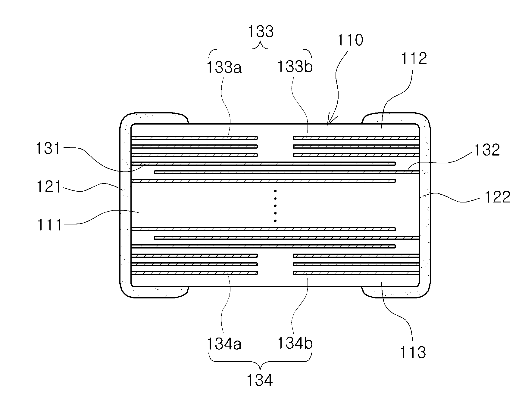
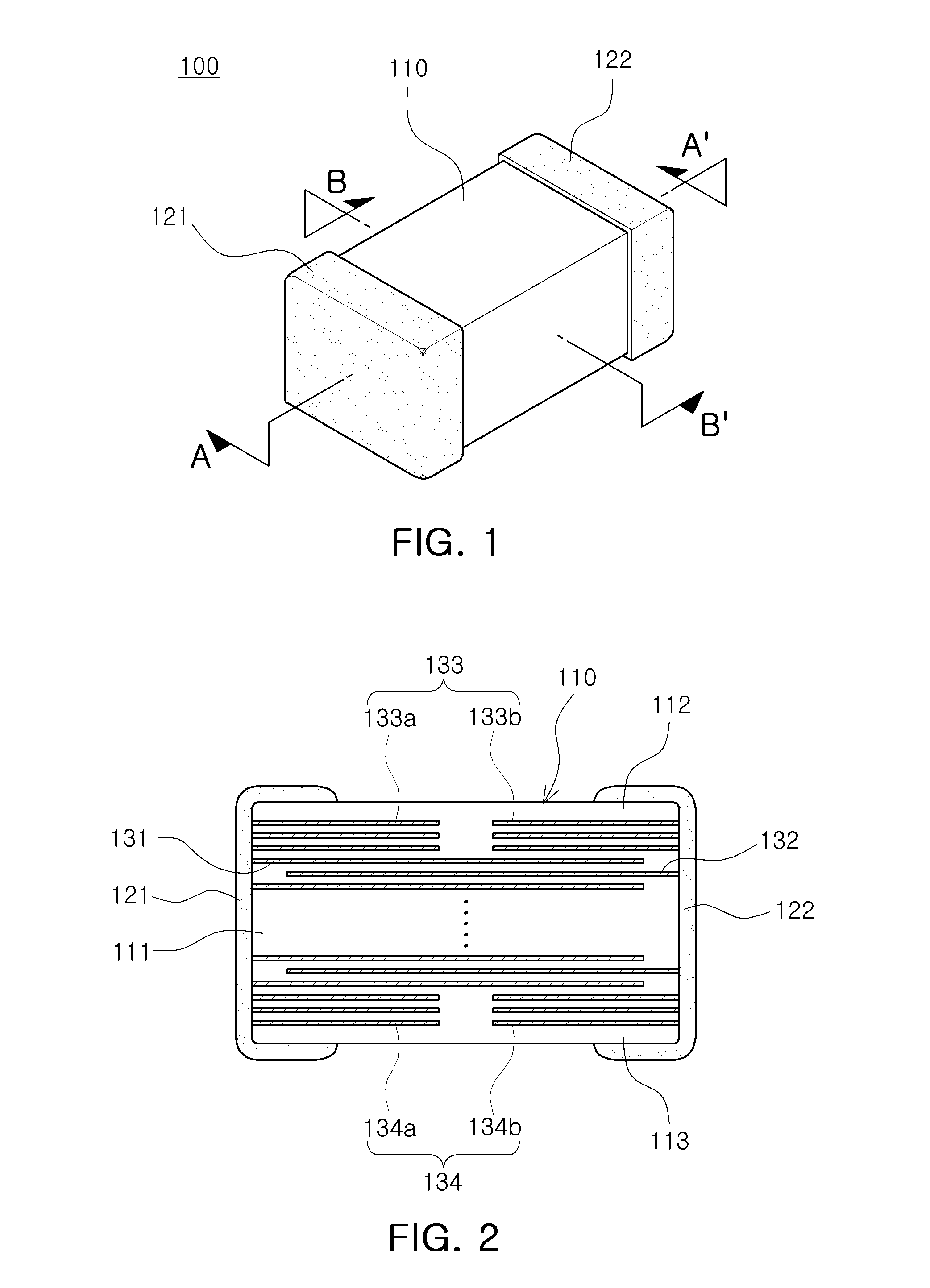
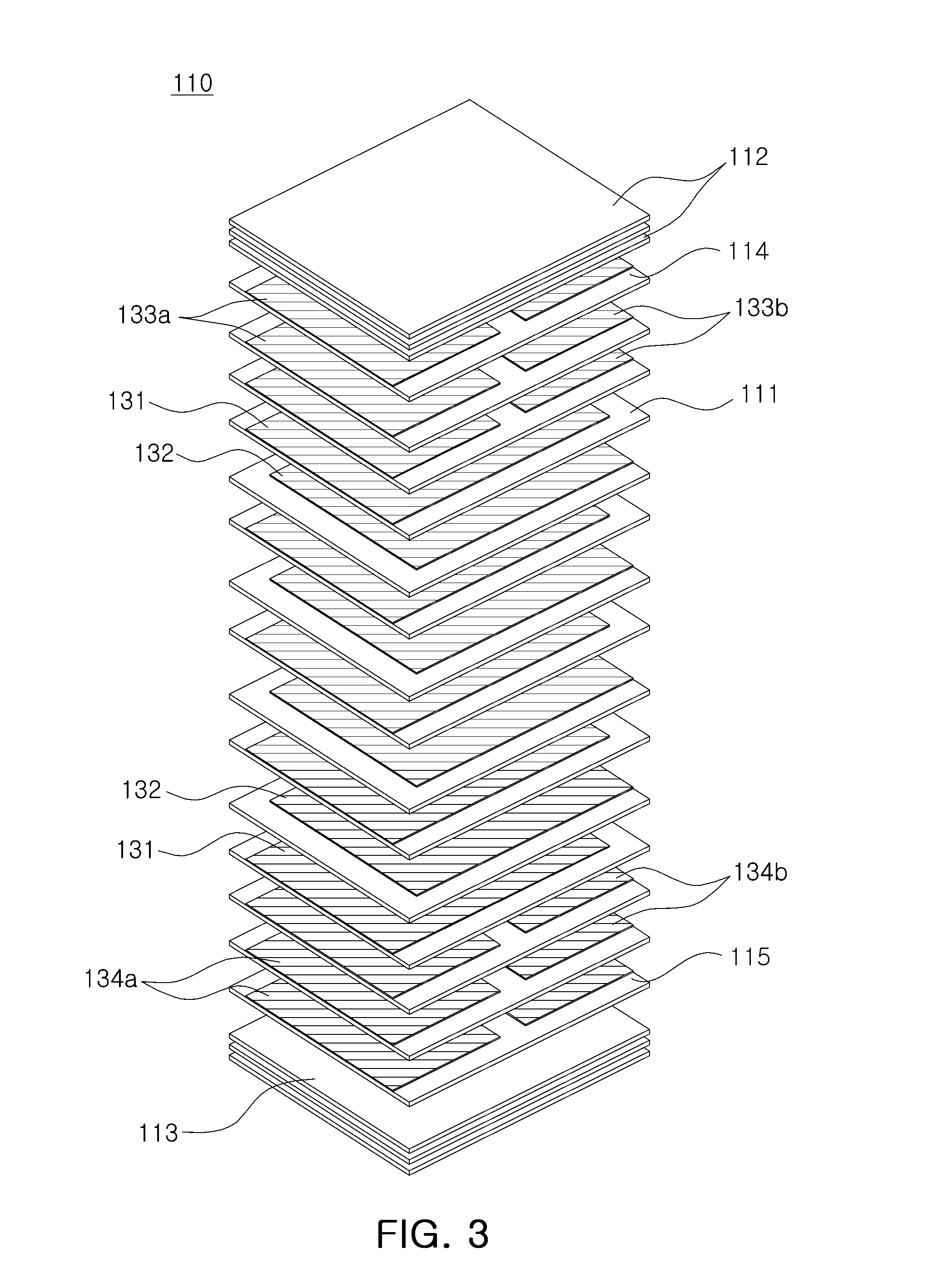
There is provided a multilayer ceramic electronic component, including: a ceramic element including a plurality of dielectric layers laminated therein; a plurality of first and second internal electrodes formed on dielectric layers positioned in a middle portion of the ceramic element and alternately exposed from both ends of the ceramic element; a plurality of dummy electrodes formed on dielectric layers positioned in upper and lower portions of the ceramic element, respectively; and first and second external electrodes formed on both ends of the ceramic element and electrically connected to the exposed portions of the first and second internal electrodes, wherein the length of each of the dummy electrodes is longer than that of the first and second external electrodes covering the ceramic element.

Description

CROSS-REFERENCE TO RELATED APPLICATIONS[0001]This application claims the priority of Korean Patent Application No. 10-2012-0025745 filed on Mar. 13, 2012, in the Korean Intellectual Property Office, the disclosure of which is incorporated herein by reference.BACKGROUND OF THE INVENTION[0002]1. Field of the Invention[0003]The present invention relates to a multilayer ceramic electronic component and a fabrication method thereof.[0004]2. Description of the Related Art[0005]Electronic components such as a capacitor, an inductor, a piezoelectric element, a varistor, a thermistor, and the like may include a ceramic material.[0006]Among ceramic electronic components, a multilayer ceramic capacitor (MLCC) is an electronic component having strengths in that it is small, has a guaranteed high capacity, and is easily mounted.[0007]Such an MLCC is a chip-type condenser mounted on a circuit board of various electronic products such as image display devices including a liquid crystal display (LC...

Claims


Application Information

Patent Timeline
Patent Type & Authority Applications(United States)
IPC IPC(8): H01L41/187B32B37/06H01G4/30H01C7/10H01F5/00
CPCH01G4/30H01F41/041H01F17/0013H01F17/04H01G4/232H01L41/083H01L41/273H01G4/012H01G4/12H01F27/292H10N30/50H10N30/053
Inventor LEE, CHUNG EUNKIM, DOO YOUNGKIM, TAE HYEOKCHOI, JAE YEOL
Owner SAMSUNG ELECTRO MECHANICS CO LTD
Why Eureka
Try Eureka