

High performance surface mount electrical interconnect
- Summary
- Abstract
- Description
- Claims
- Application Information
AI Technical Summary
Benefits of technology
Problems solved by technology
Method used
Image


Examples
Embodiment Construction
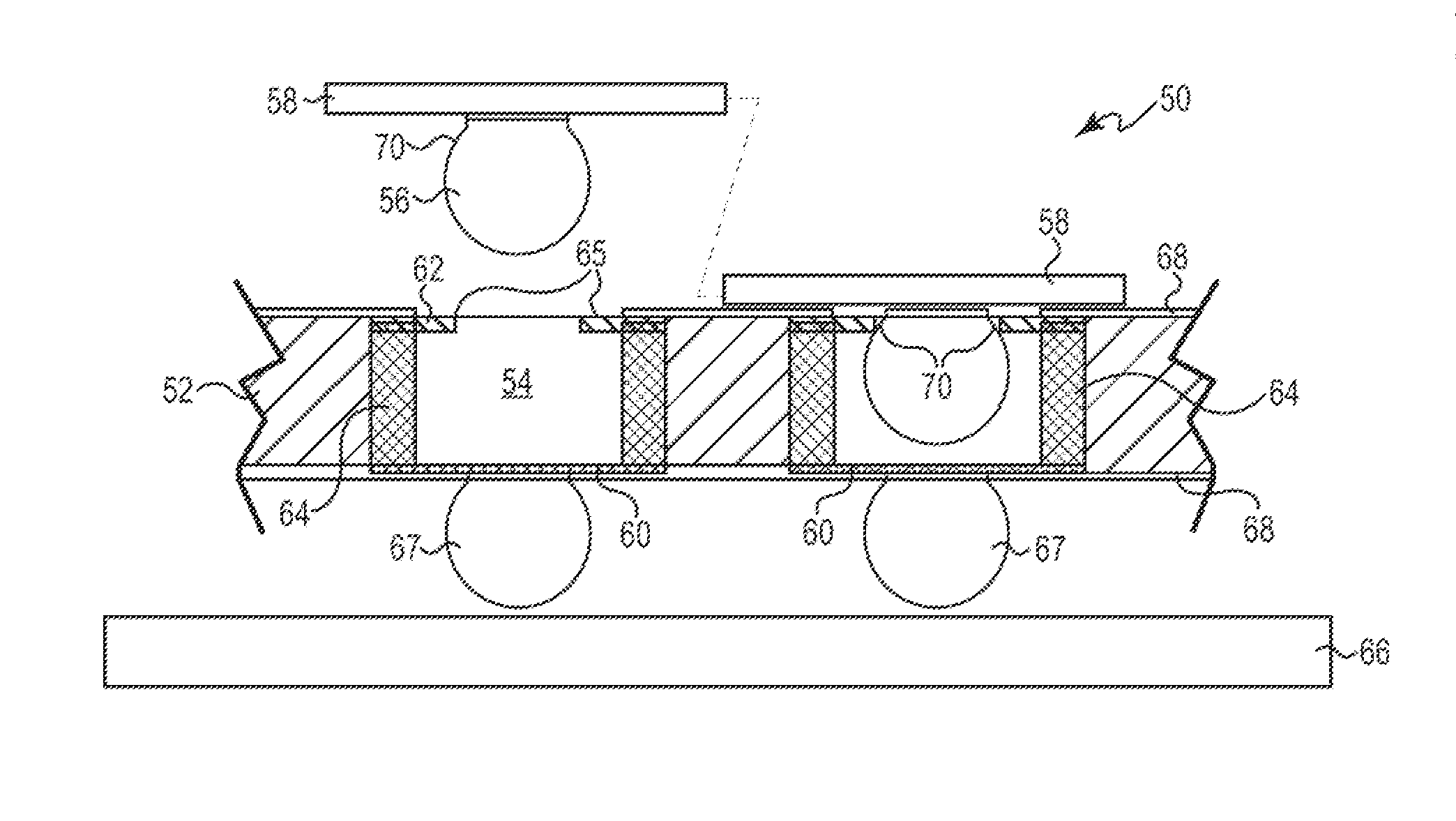
[0051]A high performance electrical interconnect according to the present disclosure may permit fine contact-to-contact spacing (pitch) on the order of less than 1.0 mm pitch, and more preferably a pitch of less than about 0.7 millimeter, and most preferably a pitch of less than about 0.4 millimeter. Such fine pitch high performance electrical interconnects are especially useful for communications, wireless, and memory devices.
[0052]The present high performance electrical interconnect can be configured as a low cost, high signal performance interconnect assembly, which has a low profile that is particularly useful for desktop and mobile PC applications. IC devices can be installed and uninstalled without the need to reflow solder. The solder-free electrical connection of the IC devices is environmentally friendly.
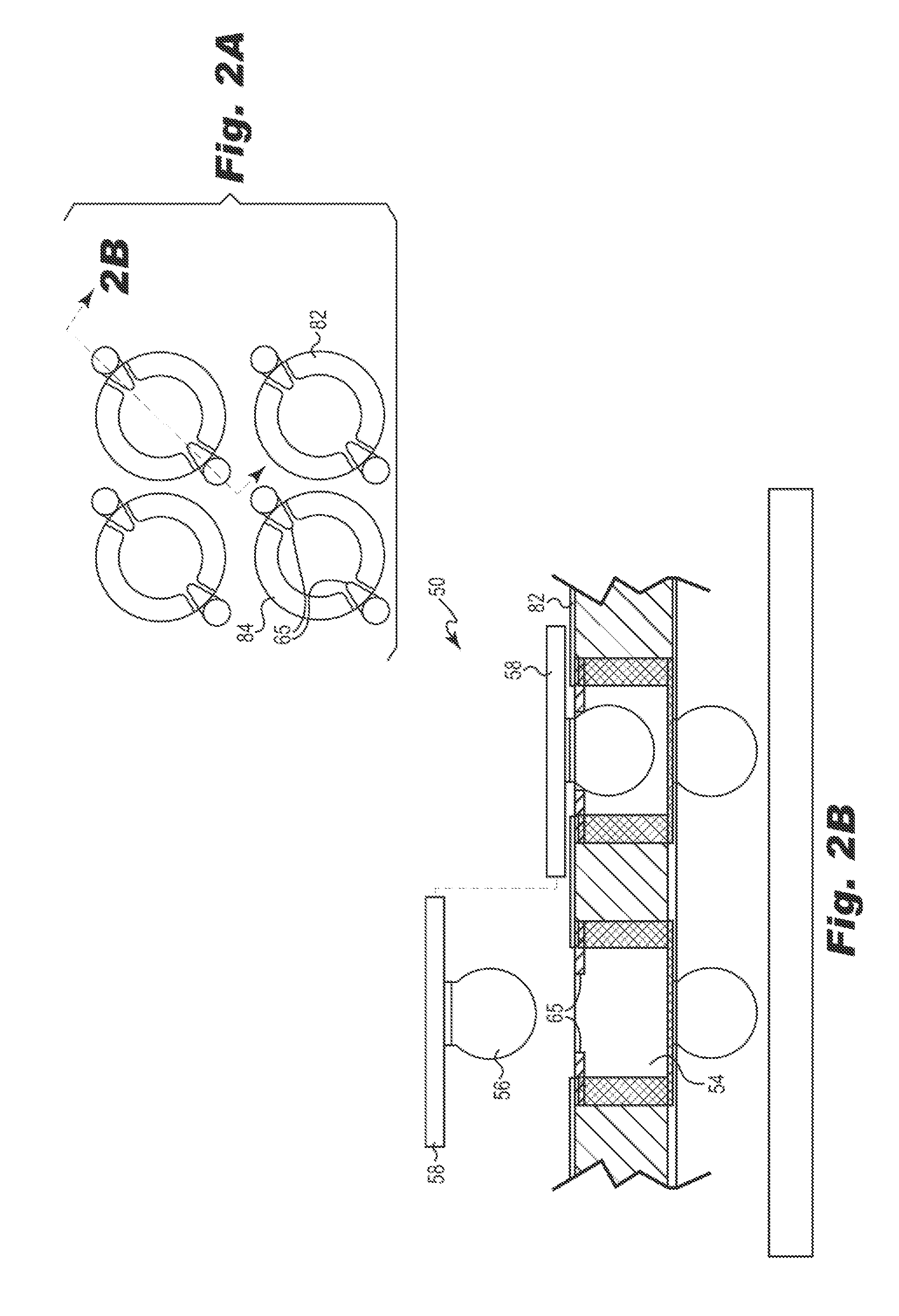
[0053]FIGS. 1A and 1B are top and cross-sectional views of a surface mount electrical interconnect 50 in accordance with an embodiment of the present disclosure. Socket sub...
PUM
| Property | Measurement | Unit |
|---|---|---|
| Dielectric polarization enthalpy | aaaaa | aaaaa |
| Electrical conductivity | aaaaa | aaaaa |
| Diameter | aaaaa | aaaaa |
Abstract
Description
Claims
Application Information