Electrical conductor and a production method therefor

a production method and technology of an electric conductor, applied in the field of electric conductors, can solve the problems of reducing the sensitivity of large-scale production, limiting the improvement of moire phenomenon, and high cost of ito film, etc., and achieves low cost, easy to perform, excellent conductivity

Active Publication Date: 2013-09-26
LG CHEM LTD
View PDF1 Cites 15 Cited by
  • Summary
  • Abstract
  • Description
  • Claims
  • Application Information

AI Technical Summary

Benefits of technology

[0019]According to the embodiments of the present invention, the electrical conductor may not obstruct the field of vision, have excellent conductivity, and prevent a Moire phenomenon. In addition, since the electrical conductor according to the present invention can be formed by using various methods such as using a printing method, a photolithography method, a photography method, a method using a mask, a sputtering method, or an inkjet method after a desired pattern is previously set, the process is easily performed and the cost is low.

Problems solved by technology

However, since a transparent conductive film has the high resistance of 100 ohms / square or more, the sensitivity is lowered when it is manufactured in a large scale.
Further, a high cost of ITO film makes the commercialization of a large-scale screen.
When a display device includes an electromagnetic wave shield film or a touch panel that includes a metal pattern, a Moire phenomenon may be caused by the interference between the metal pattern and a pixel pattern of the display, electrode pattern or pattern structure of the other optical film.
In order to remove a Moire phenomenon, the line width and pitch and angle of the metal mesh pattern for the electromagnetic wave shielding are controlled, but there is a problem in that it should correspond to different patterns according to the size and the pixel implementation method of the display device.
Accordingly, there is a limit in improvement of the Moire phenomenon by using only the line width, pitch, and angle of the known pattern.

Method used


Image

  • Electrical conductor and a production method therefor
  • Electrical conductor and a production method therefor
  • Electrical conductor and a production method therefor

Examples


example

Example 1

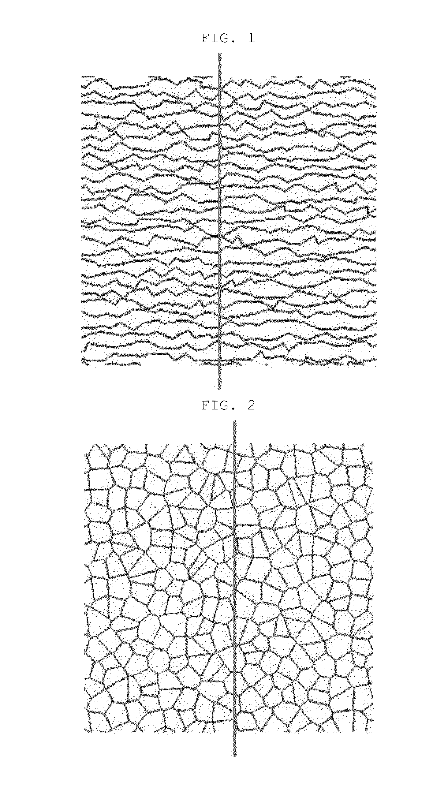
[0123]The silver paste was manufactured by dissolving 80 wt % of silver particles that had the particle diameter of 2 micrometers, 5 wt % of polyester resin, and 5 wt % of grass frit in 10 wt % of the BCA (butyl carbitol acetate) solvent. As the intaglio printing plate, the glass that had the width of 20 micrometers, the depth of 7.5 micrometers, and the average interval between lines of 600 micrometers and the same pattern as FIG. 1 was used. In this case, when the straight line that crossed the formed pattern was drawn, the ratio (distance distribution ratio) of standard deviation in respect to an average value of distances between adjacent intersection points of the straight line and the pattern was about 30%.

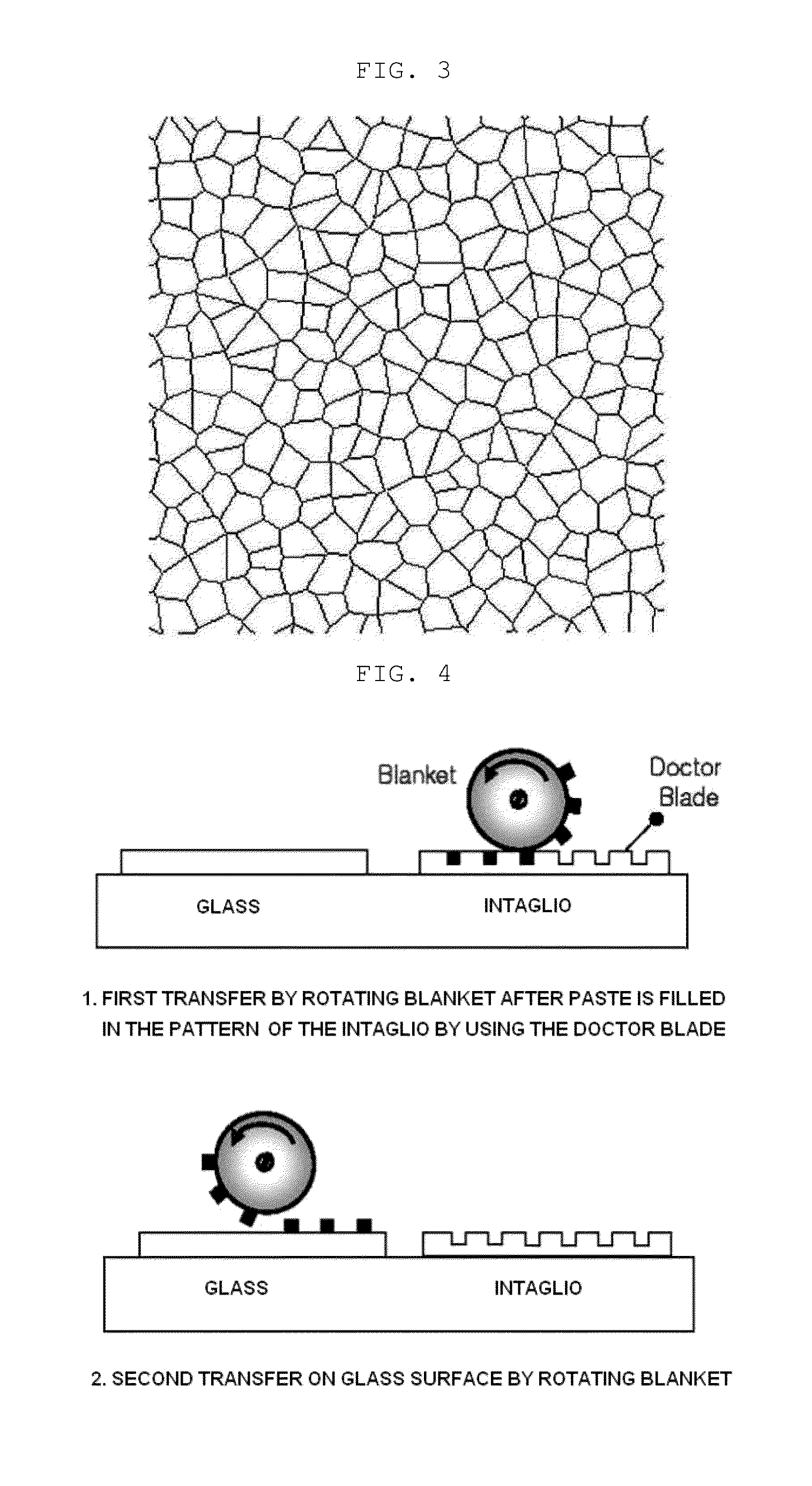
[0124]After the silver pattern was formed on the glass substrate by using the method shown in FIG. 4 and the offset printer, the silver pattern was sintered at 600° C. for 3 min to form the pattern shown in FIG. 1.

[0125]The surface resistance of the glass substrate ...

example 2

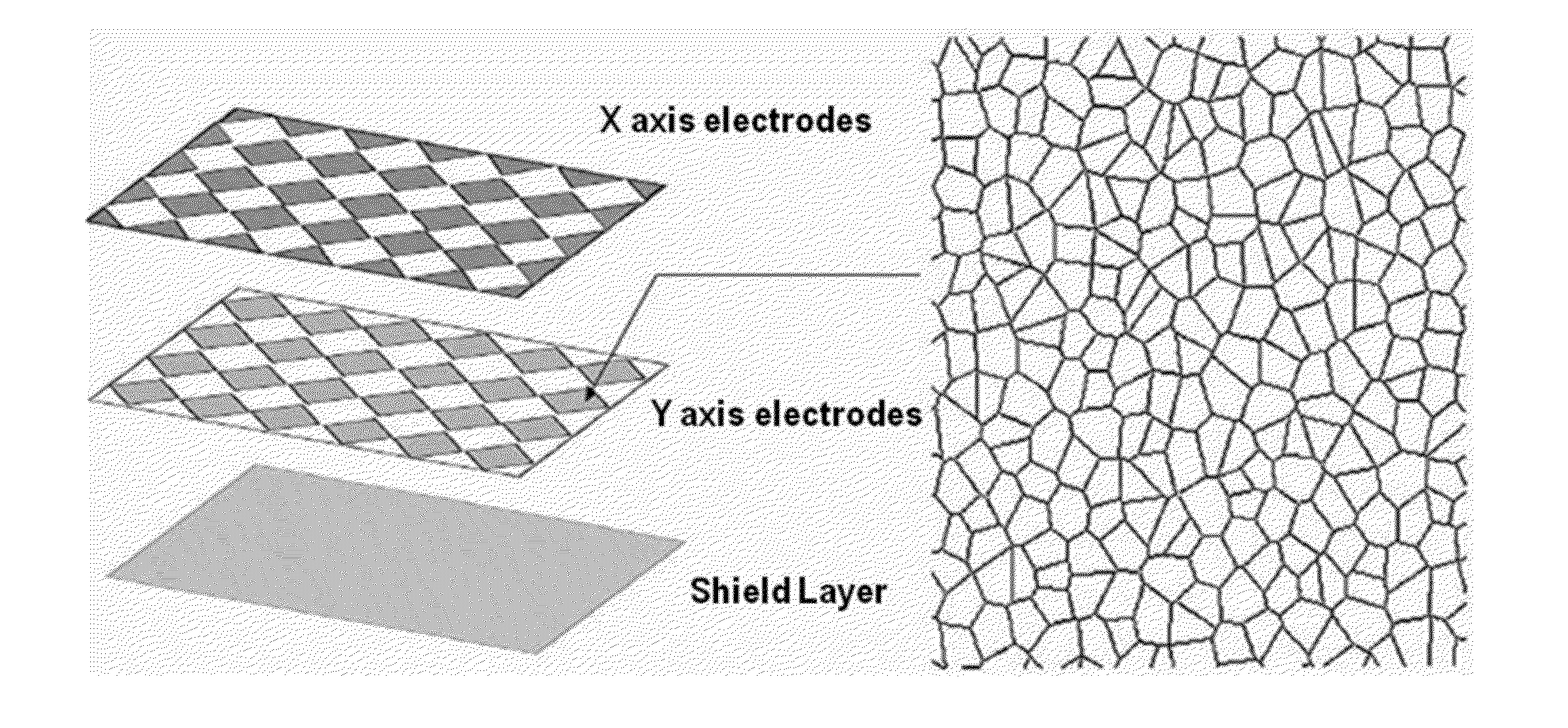
[0128]The silver paste was manufactured by dissolving 80 wt % of silver particles that had the particle diameter of 2 micrometers, 5 wt % of polyester resin, and 5 wt % of grass frit in 10 wt % of the BCA (butyl carbitol acetate) solvent. As the intaglio printing plate, the glass that had the width of 20 micrometers, the depth of 7.5 micrometers and the same pattern as FIG. 6 was used.

[0129]After the silver pattern was formed on the glass substrate (100 mm×100 mm) by using the method shown in FIG. 3 and the offset printer, the silver pattern was sintered at 600° C. for about 3 min to form the pattern shown in FIG. 6. In this case, when the straight line that crossed the formed pattern was drawn, the ratio (distance distribution ratio) of standard deviation in respect to an average value of distances between adjacent intersection points of the straight line and the pattern was about 50%.

[0130]The 40-inch PDP was manufactured by using the glass substrate, and the Moire phenomenon ther...

example 3

[0135]The photosensitive material for negative was coated on the PET film substrate on which the pattern will be formed. The photosensitive material for negative was formed of silver halide in which AgBr that was very sensitive to and regularly reacted with light and a small amount of AgI were mixed with each other. The irregular pattern that was formed on the PET film substrate was the same as the pattern of Example 1. By using the negative mask that was configured so that light penetrates the designed pattern area and light does not penetrate an area other than the pattern, light was irradiated to the film according to the set exposure time and intensity of light. By this process, photosensitive silver on the photosensitive emulsion layer was photosensitized to form a latent image. Photosensitive silver was converted into blackened silver through the development process of the formed latent image, such that the reverse image pattern of the mask pattern was formed in a visible phas...


PUM

PropertyMeasurementUnit
transparentaaaaaaaaaa
heightaaaaaaaaaa
heightaaaaaaaaaa

Abstract

Provided are an electrical conductor and a production method therefor; the electrical conductor comprising a transparent substrate and an electro-conductive pattern provided on at least one surface of the transparent substrate, and the electroconductive pattern being of a type such that, for at least 30% of the entire surface area of the transparent substrate, when a straight line is drawn intersecting the electroconductive pattern, the ratio of the standard deviation to the mean value of the distances between adjacent points of intersection between the straight line and the electroconductive pattern (the distance distribution ratio) is at least 2%. Also, provided are an electrical conductor and a production method therefor; the electrical conductor comprising a transparent substrate and an electroconductive pattern provided on at least one surface of the transparent substrate, and the electroconductive pattern being of a type such that at least 30% of the entire surface area of the transparent substrate is accounted for by continuously distributed closed motifs, and the ratio of the standard deviation to the mean value of the surface areas of the closed motifs (the surface area distribution ratio) is at least 2%.

Description

TECHNICAL FIELD[0001]The present invention relates to an electrical conductor and a production method therefor.[0002]The present application claims priority to Korean Patent Application Nos. 10-2009-0065103 and 10-2009-0065106 filed on Jul. 16, 2009 and Korean Patent Application No. 10-2010-0069157 filed on Jul. 16, 2010, the entire contents of which application is incorporated herein for all purposes by this reference.BACKGROUND OF THE INVENTION[0003]In general, a display device is monitors for TV or computers, and includes a display diode that forms an image and a case that supports the display diode.[0004]As a display diode, there may be exemplified by plasma display panel (PDP), liquid crystal display (LCD), electrophoretic display and cathode-ray tube (CRT). In a display diode, an RGB pixel pattern and additional optical filter for implementing an image may be provided.[0005]An optical filter may include at least one of an anti-reflective film that prevents the reflection of th...

Claims


Application Information

Patent Timeline
Patent Type & Authority Applications(United States)
IPC IPC(8): H05K1/02H05K9/00H05K3/10
CPCH01L51/5212H05K1/0296H05K3/10H05K9/0064Y10T29/49155G06F3/044G06F2203/04103G06F2203/04112G06F3/041G06F3/0445G06F3/0412H10K59/80516H10K50/814
Inventor LEE, DONG-WOOKHWANG, IN-SEOKCHUN, SANG-KIHWANG, JI-YOUNGCHOI, HYEONHONG, YOUNG-JUNKIM, SU-JINKIM, KI-HWAN
Owner LG CHEM LTD
Why Eureka
Try Eureka