Electromagnetic casting method and apparatus for polycrystalline silicon

a technology of polycrystalline silicon and electromagnetism, which is applied in the direction of glass tempering apparatus, instruments, manufacturing tools, etc., can solve the problems of affecting the production yield of ingots, so as to prevent the confluence of molten silicon inside the solidified portion and prevent the cracking of ingots. , the effect of preventing the cracking

Active Publication Date: 2013-10-03
SUMCO CORP
View PDF7 Cites 4 Cited by
  • Summary
  • Abstract
  • Description
  • Claims
  • Application Information

AI Technical Summary

Benefits of technology

[0031]According to the electromagnetic casting method of polycrystalline silicon, a precipitation region of foreign substances can be limited in a finally solidified portion of ingot, and the confinement of molten silicon inside the solidified portion can be prevented. Therefore, a production yield of ingot can be improved by preventing cracking of ingot as well as by reducing a precipitation region of foreign substances and a region where crystal defects being generated that are attributed to the above. This method can be easily performed by using the electromagnetic casting apparatus for polycrystalline silicon of the invention.

Problems solved by technology

In this operation, if the liquid molten silicon should be left in as-is condition, solidification should start from the upper surface of the molten silicon in the mold, the molten silicon confined therein should be solidified in the final phase, and thus cracking is liable to occur in the finally solidified portion of the ingot due to a volume expansion associated with the final solidification.
However, in this final solidification process, the following two problems occasionally arise.
One problem is that after the plasma arc heating is stopped, the precipitation of foreign substances is caused by an abrupt temperature drop before starting to warm the molten silicon by the carbon block.
These impurities cause a leak current failure called a shunt when a solar cell was made using a wafer cut from a silicon ingot including these impunities as a substrate.
The other problem, which may be caused in the final solidification process, is that the ingot is broken by a solidification expansion when the surface only is solidified earlier while the molten silicon is confined inside the solidified portion.
No cases of preventive measures have been reported so far with respect to such the precipitation of foreign substances or cracking in a finally solidified portion of silicon ingot.
However, the precipitation of foreign substances in the finally solidified portion of ingot, a crystalline quality degradation caused therefrom, cracking generation, and counter measures against these problems are not described in JP-A No. 2001-19593.

Method used


Image

  • Electromagnetic casting method and apparatus for polycrystalline silicon
  • Electromagnetic casting method and apparatus for polycrystalline silicon
  • Electromagnetic casting method and apparatus for polycrystalline silicon

Examples


examples

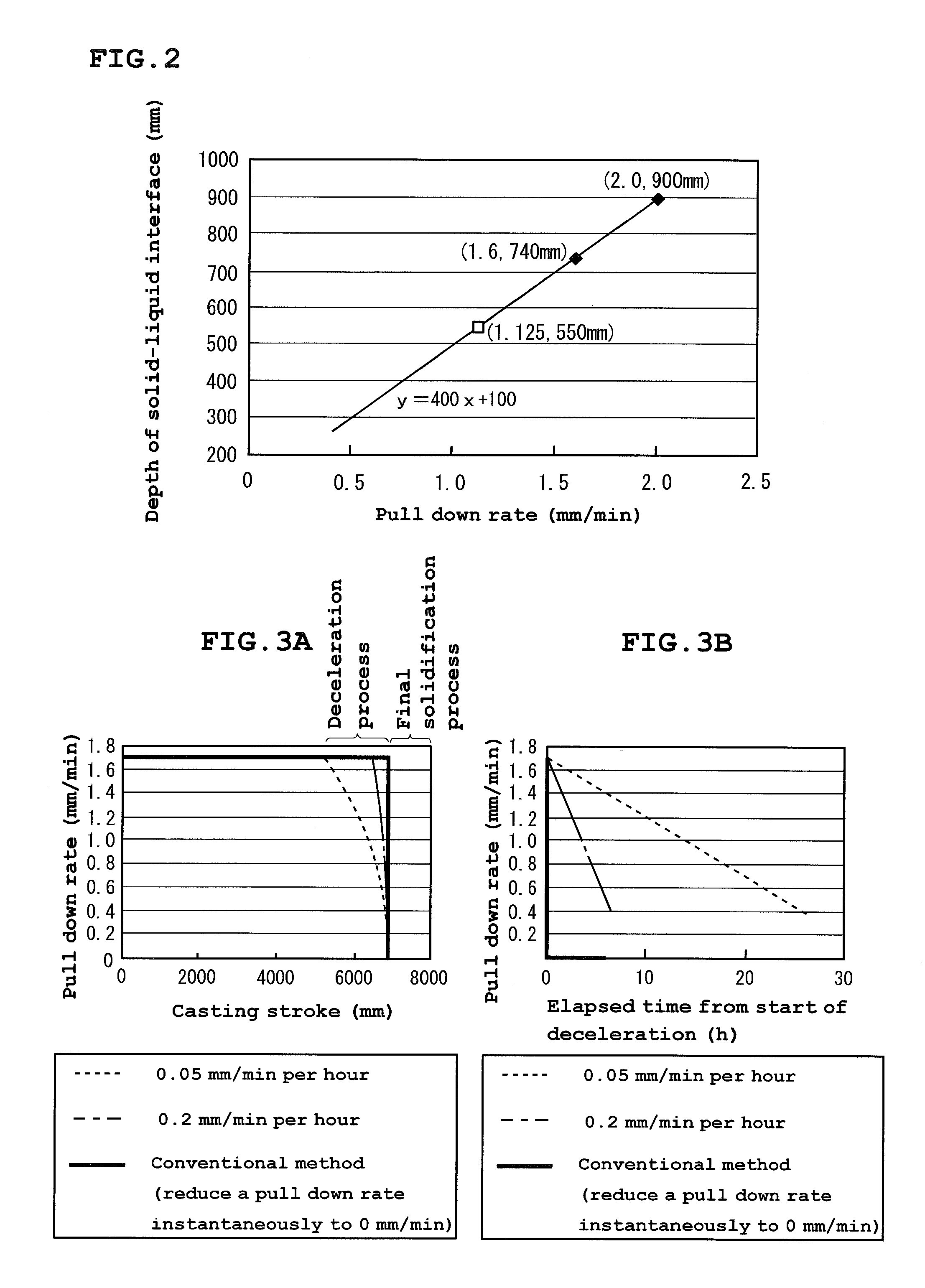
[0062]By using an apparatus having a configuration described in FIG. 1 above, and applying an electromagnetic casting method of the invention, a silicon ingot (sectional shape: 345 mm×512 mm, length: 6,900 mm) was cast to examine the region of precipitation of foreign substances and the absence or presence of cracking generation in the finally solidified portion of ingot. For comparison, a similar examination was also performed in a case of applying a conventional casting method in which a pull down rate was not reduced.

[0063]As described below, casting conditions were the same as those illustrated in FIGS. 3A and 3B above.

Condition 1: Decelerate at a rate of 0.05 mm / min per hour from a casting stroke of 5,222.0 mm

Condition 2: Decelerate at a rate of 0.2 mm / min per hour from a casting stroke of 6,450.5 mm

Conventional method: Decelerate immediately to 0 mm / min at a casting stroke of 6,860 mm

[0064]Methods for measuring and evaluating the region of precipitation of foreign substances a...


PUM

PropertyMeasurementUnit
lengthaaaaaaaaaa
depthaaaaaaaaaa
depthaaaaaaaaaa

Abstract

Disclosed is an electromagnetic casting method of polycrystalline silicon which is characterized in that polycrystalline silicon is continuously cast by charging silicon raw materials into a bottomless cold mold, melting the silicon raw materials using electromagnetic induction heating, and pulling down the molten silicon to solidify it, wherein the depth of solid-liquid interface before the start of the final solidification process is decreased by reducing a pull down rate of ingot in a final phase of steady-state casting. By adopting the method, the region of precipitation of foreign substances in the finally solidified portion of ingot can be reduced and cracking generation can be prevented upon production of a polycrystalline silicon as a substrate material for a solar cell.

Description

BACKGROUND OF THE INVENTION[0001]1. Field of the Invention[0002]The present invention relates to an electromagnetic casting method and apparatus for continuously producing a polycrystalline silicon ingot by applying a casting technique through electromagnetic induction, particularly, an electromagnetic casting method of silicon capable of preventing a crack generation by reducing the region of precipitation of foreign substances in a finally solidified portion of the silicon ingot upon production of a polycrystalline silicon to be used as a substrate material of a solar cell, and an electromagnetic casting apparatus suitable for conducting the same.[0003]2. Description of the Related Art[0004]When an electromagnetic casting apparatus, to which a bottomless cold mold divided in a circumferential direction is attached, is used, since a molten substance (molten silicon in this case) and the mold are almost non-contact with each other, a silicon ingot free of impurity contamination can ...

Claims


Application Information

Patent Timeline
Patent Type & Authority Applications(United States)
IPC IPC(8): H01L31/028
CPCC30B29/06H01L31/028C30B13/20C30B15/08C30B28/06B22D11/20B22D11/041B22D11/108B22D11/11B22D11/1213B22D11/001Y02E10/547C30B28/04
Inventor MAEGAWA, KOICHIONIZUKA, TOMOHIROYOSHIHARA, MITSUO
Owner SUMCO CORP
Why Eureka
Try Eureka