Method for applying power to target material, power supply for target material, and semiconductor processing apparatus

a technology of target material and power supply, applied in the field of microelectronics, can solve the problems of inability to meet the requirements of the technology and apparatus in the art, the method of enhancing the metal ionization rate by increasing the magnetic field intensity is limited, and the material depositing speed is too fast, so as to improve the metal ionization rate of the sputtering process, the effect of ensuring process stability and controllability

Inactive Publication Date: 2013-10-03
BEIJING NAURA MICROELECTRONICS EQUIP CO LTD
View PDF3 Cites 3 Cited by
  • Summary
  • Abstract
  • Description
  • Claims
  • Application Information

AI Technical Summary

Benefits of technology

[0023]As another technical solution, the semiconductor processing apparatus provided by the present invention adopts the above method for applying power to target material provided by the present invention or connects the power supply for target material provided by the present invention to the target material during a magnetron sputtering process, and it can effectively enhance the metal ionization rate of sputtering process in case that the process stability and controllability are guaranteed, thus the requirement of new technology node is satisfied.

Problems solved by technology

However, magnetic field intensity of any material has a particular physical limit, thus, the method of enhancing the metal ionization rate by increasing the magnetic field intensity is limited.
Moreover, continually applying a high magnetic field intensity and a high DC power will result in a problem that a depositing speed of material is too fast, while too fast depositing speed will increase the difficulty to control result of a deposition process, and thus result in a disadvantageous process result.
However, such requirement could not be satisfied in view of the technology and apparatus in the art.

Method used


Image

  • Method for applying power to target material, power supply for target material, and semiconductor processing apparatus
  • Method for applying power to target material, power supply for target material, and semiconductor processing apparatus
  • Method for applying power to target material, power supply for target material, and semiconductor processing apparatus

Examples


Embodiment Construction

[0030]For better understanding of the technical solution of the present invention by the persons skilled in the art, a method for applying power to target material, a power supply for target material, as well as a semiconductor processing apparatus adopting the above method for applying power to target material / power supply for target material provided by the present invention will be described in detail by reference to the drawings.

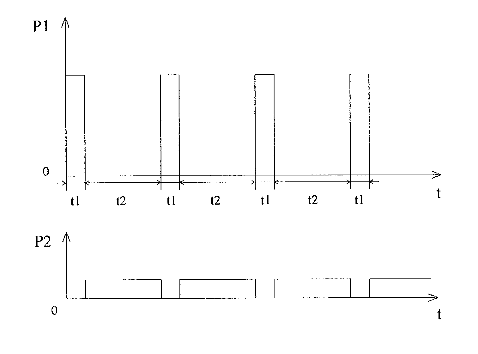
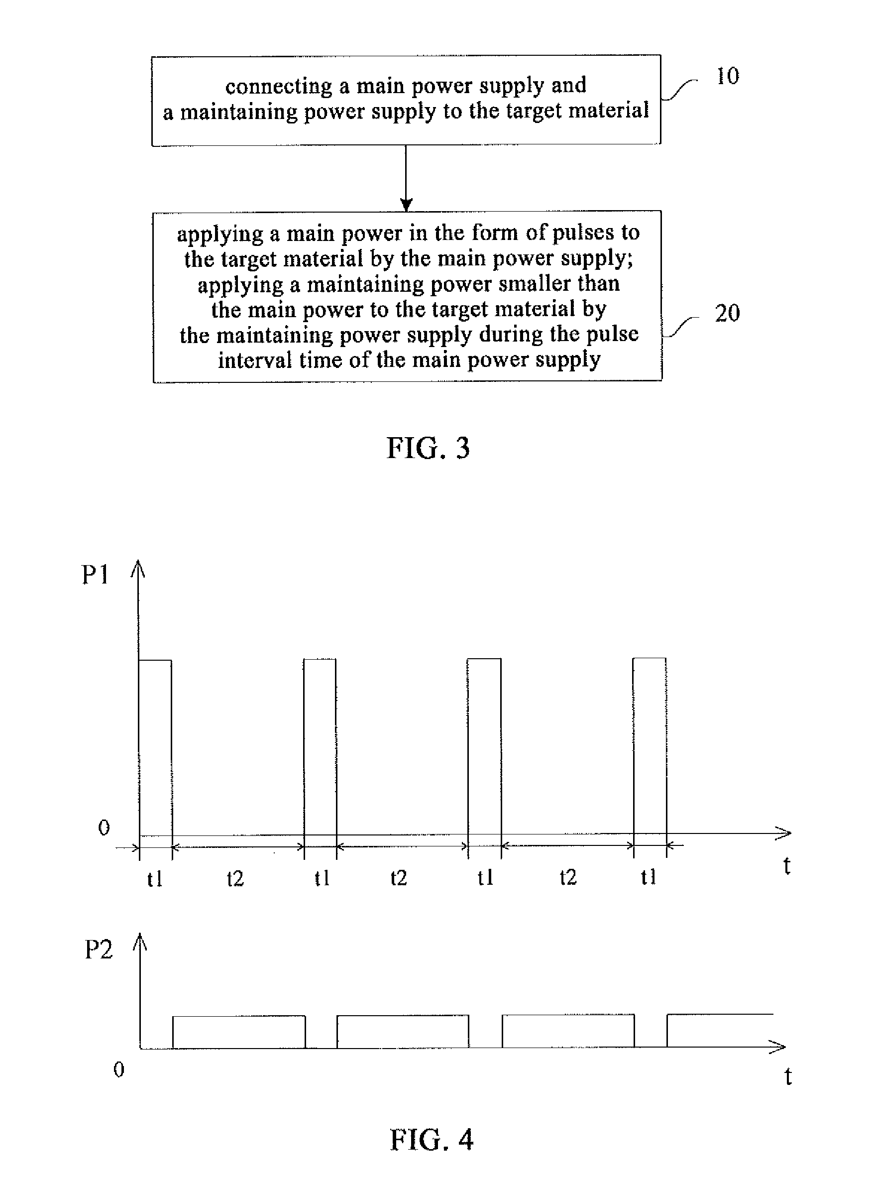
[0031]FIG. 3 is a flow chart of a method for applying power to target material provided by the present invention. The method for applying power to target material is mainly used for applying power to the target material during a magnetron sputtering process, and includes the following steps: 10) connecting a main power supply and a maintaining power supply to the target material respectively; 20) applying a particular main power in the form of pulses to the target material by the main power supply, wherein the active time of a singe pulse is t1, and the ...


PUM

PropertyMeasurementUnit
frequencyaaaaaaaaaa
poweraaaaaaaaaa
timeaaaaaaaaaa

Abstract

A method for applying power to target material in a magnetron sputtering process is provided. The method includes: 10) connecting a main power supply and a maintaining power supply to the target material (2) respectively; 20) applying a particular main power in the form of pulses to the target material (2) by the main power supply; applying a particular maintaining power which is smaller than the main power to the target material (2) by the maintaining power supply at least during the pulse interval time (t2) of the main power supply, so as to maintain a glow discharge procedure of the sputtering process during the purse interval time (t2) of the main power supply. The method for applying power to target material can obviously enhance the metal ionization rate while the process stability and controllability are guaranteed. A power supply for target material (8) which includes a main power module (81) and a maintaining power module (82), and a semiconductor processing apparatus using the method for applying power to target material or the power supply for target material are also provided.

Description

TECHNICAL FIELD[0001]The present invention relates to a technical field of micro-electronics, particularly to a method for applying power to target material, a power supply for target material, as well as a semiconductor processing apparatus using the method for applying power to target material / the power supply for target material.BACKGROUND[0002]In modern industry, the micro-electronics processing technology has obtained great achievement. Wherein, large scale integrated circuits (ICs) have been widely used in various fields of production and life of people. Meantime, manufacturing process and process apparatus for integrated circuits are continuously improved and updated in an amazing speed.[0003]Magnetron sputtering is a key technology used for manufacturing an interconnection layer of metal such as copper / aluminum in an integrated circuit. In the process of magnetron sputtering, part of atoms of target material are sputtered out in ion state from a surface of the target materia...

Claims


Application Information

Patent Timeline
Patent Type & Authority Applications(United States)
IPC IPC(8): C23C14/34
CPCC23C14/3485H01J37/3408H01J37/3467C23C14/35
Inventor YANG, BAIXIA, WEI
Owner BEIJING NAURA MICROELECTRONICS EQUIP CO LTD
Why Eureka
Try Eureka