Dual source follower pixel cell architecture

a follower pixel and dual source technology, applied in the field of image sensors, can solve the problems of reducing the uniformity of such a concentration, increasing the likelihood of charge trapping/releasing, and comparatively less uniform concentration of dopant in the active area

Inactive Publication Date: 2013-10-03
OMNIVISION TECH INC
View PDF2 Cites 25 Cited by
  • Summary
  • Abstract
  • Description
  • Claims
  • Application Information

AI Technical Summary

Problems solved by technology

However, some later stage in pixel cell fabrication may reduce the uniformity of such a dopant concentration.
Consequently, a comparatively less uniform dopant concentration in the active area may result, where the dopant concentration at a location closer to the middle of an active area tends to be higher than the active area dopant concentration at a location which is closer to an adjoining isolation structure.
Current being carr...

Method used


Image

  • Dual source follower pixel cell architecture
  • Dual source follower pixel cell architecture
  • Dual source follower pixel cell architecture

Examples


Embodiment Construction

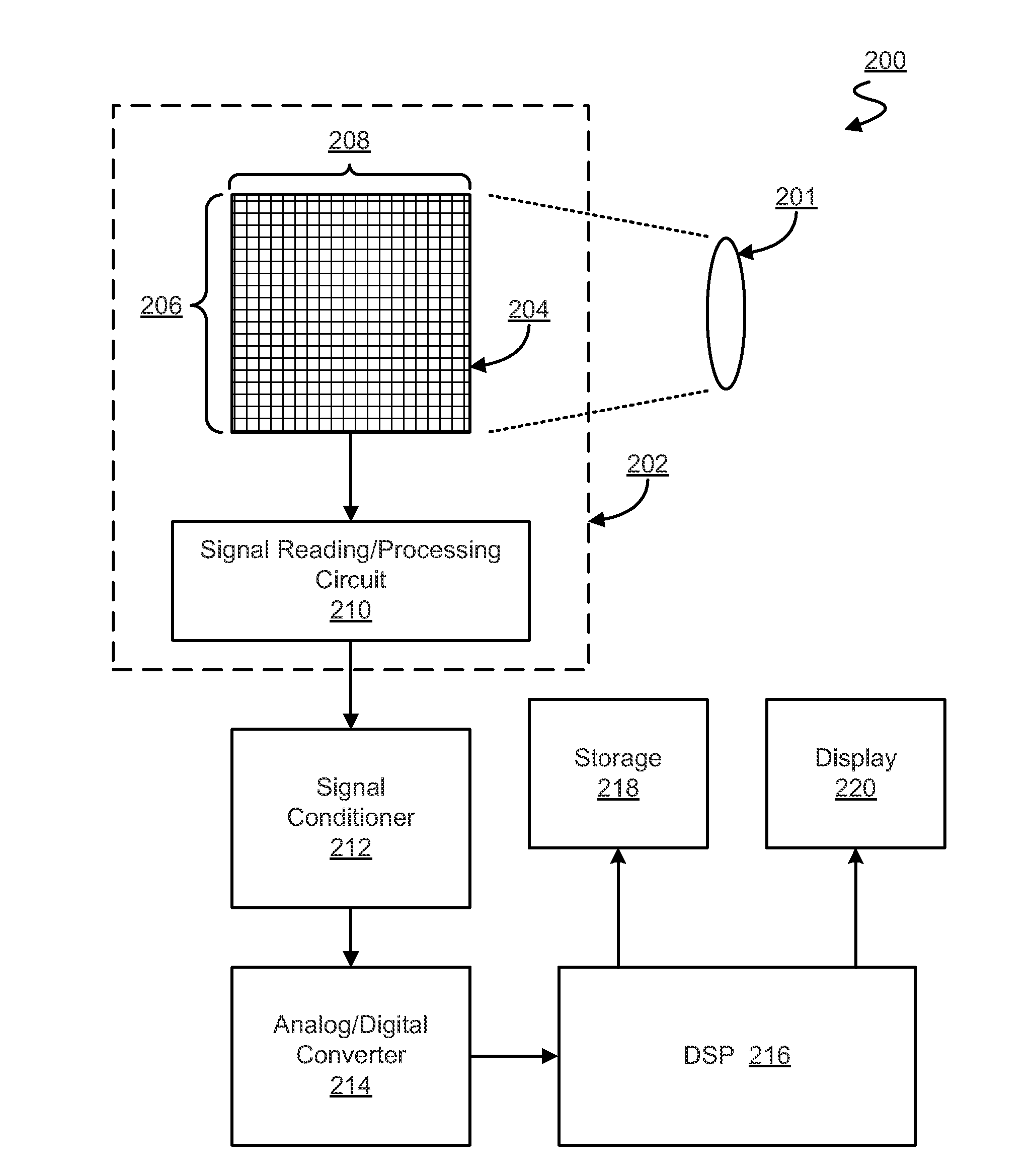
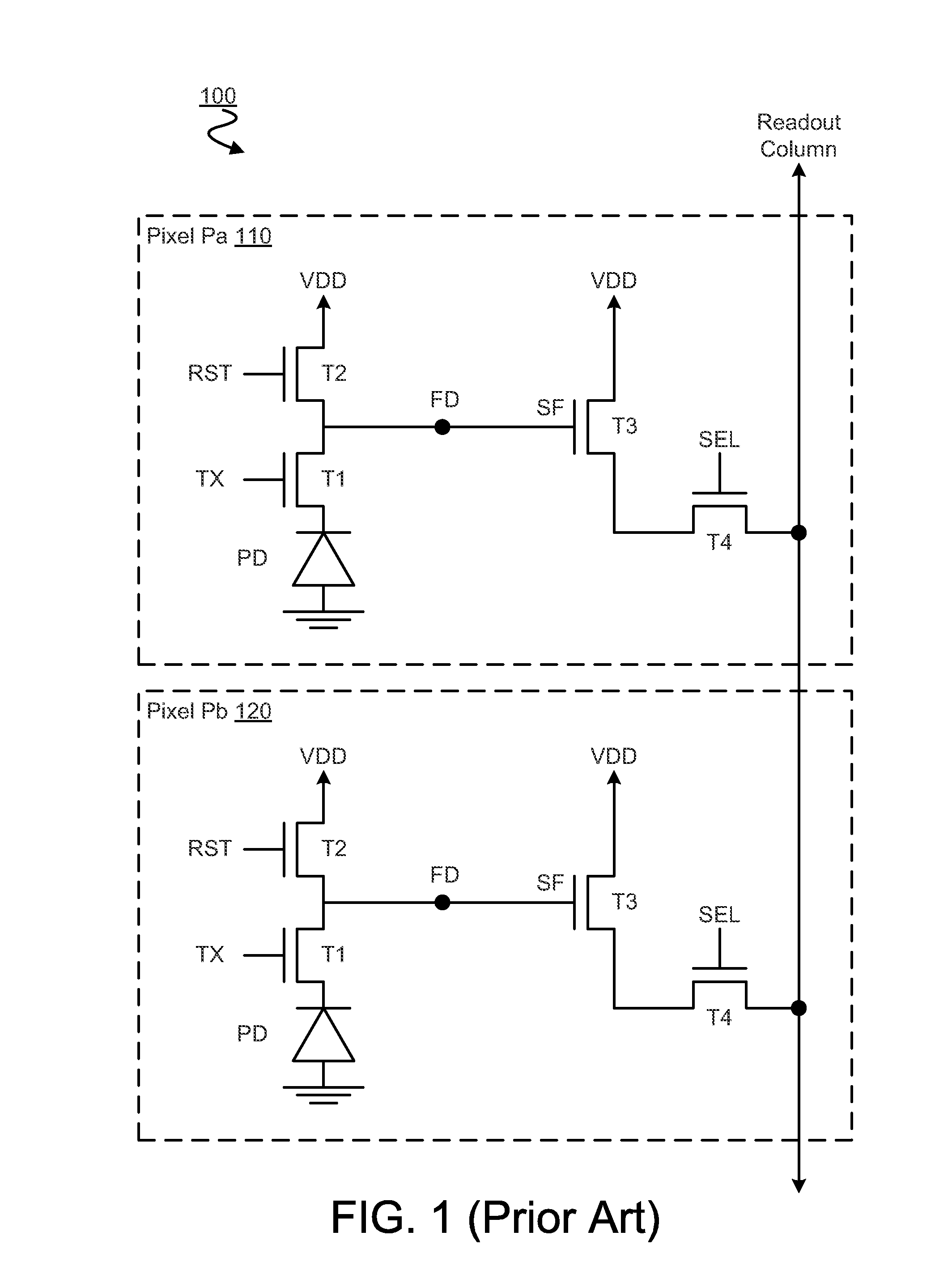
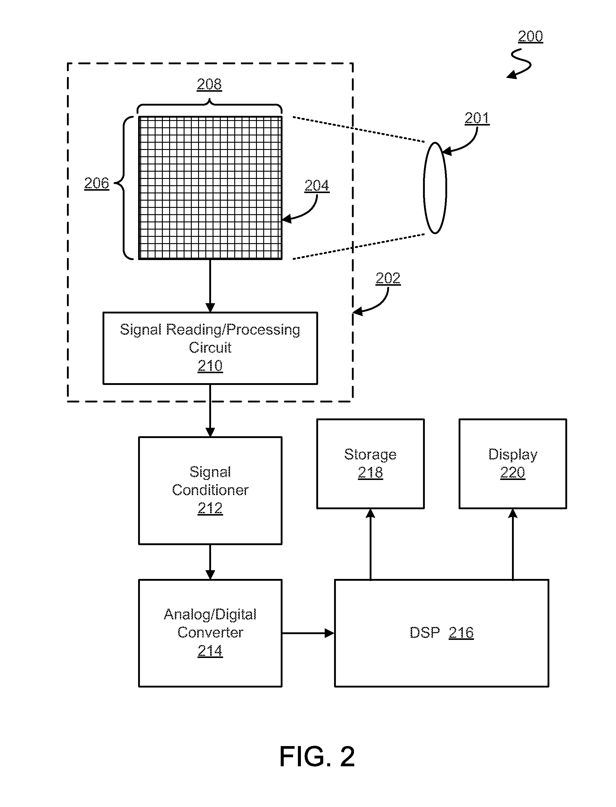
[0017]Certain embodiments discussed herein variously provide for a pixel cell architecture including two source follower transistors, each to contribute to an amplification signal of the pixel cell. A pair of source follower transistors of a pixel cell may, for example, be coupled in parallel with one another, where the respective gates of the source follower transistors are each coupled to a floating diffusion node of the pixel cell. In such an embodiment, operation of the dual source follower transistors may be based on the floating diffusion node transitioning to a voltage level corresponding to an amount of charge accumulated in a photodiode of the pixel cell. Parallel source follower transistors of a pixel cell may, in an embodiment, share an active area (e.g. including a diffusion well or other such structure) in a semiconductor substrate for the pixel cell—e.g. where respective structures of the first and second source follower transistors are variously formed in and / or on ...


PUM


Abstract

Techniques for providing a pixel cell which includes two source follower transistors. In an embodiment, a first source follower transistor of a pixel cell and a second source follower transistor of the pixel cell are coupled in parallel with one another, where the source follower transistors are each coupled via their respective gates to a floating diffusion node of the pixel cell. In another embodiment, the first source follower transistor and second source follower transistor each operate based on a voltage of the floating diffusion node to provide a respective component of an amplification signal, where the pixel cell outputs an analog signal based on the amplification signal.

Description

BACKGROUND OF THE INVENTION[0001]1. Field of the Invention[0002]This disclosure relates generally to image sensors, and in particular but not exclusively, relates to CMOS image sensors.[0003]2. Background Art[0004]Image sensors have become ubiquitous. They are widely used in digital still cameras, cellular phones, security cameras, as well as medical, automobile, and other applications. The demands of higher resolution and lower power consumption have encouraged further miniaturization and integration of these image sensors. As a result, technology used to manufacture image sensors, for example, CMOS image sensors (“CIS”), has continued to advance at a great pace.[0005]FIG. 1 is a circuit diagram showing pixel circuitry 100 including two four-transistor (“4T”) pixel cells—Pa 110 and Pb 120—of a conventional pixel array. In FIG. 1, pixel cells Pa 110 and Pb 120 are arranged in two rows and one column. Pa 110 and Pb 120 each include the same conventional pixel cell architecture in whi...

Claims


Application Information

Patent Timeline
IPC IPC(8): H01L27/148
CPCH01L27/14612H01L27/14621H01L27/14627H04N5/3745H04N5/357H04N5/361H01L27/14643H04N25/60H04N25/63H04N25/77
Inventor YANG, CUNYURHODES, HOWARD E.
Owner OMNIVISION TECH INC
Why Eureka
Try Eureka