Current correction circuit for power semiconductor device and current correction method

a technology of current correction circuit and power semiconductor device, which is applied in the direction of pulse technique, process and machine control, instruments, etc., can solve the problems of increasing the size of the detector, reducing the size of the power conversion device, and the device is expensive, so as to improve the accuracy of current detection. , the effect of high accuracy

Active Publication Date: 2013-10-03
FUJI ELECTRIC CO LTD
View PDF0 Cites 25 Cited by
  • Summary
  • Abstract
  • Description
  • Claims
  • Application Information

AI Technical Summary

Benefits of technology

[0022]According to the current correction circuit for a power semiconductor device of the invention, when the current sense ratio of a power semiconductor device with a sensing function is corrected, it is possible to automatically change an appropriate correction value according to the temperature and improve current detection accuracy in the wide temperature range since the current detecting circuit includes the temperature detecting unit and the correction unit that calculates a correction value for correcting a variation in the current sense ratio according to the detected temperature. In addition, since the amount of correction is appropriately changed according to a variation in the ambient temperature of the device, it is possible to detect the main current in the wide temperature range with high accuracy.
[0023]Furthermore, according to a current correction method for a power semiconductor device of the invention, it is possible to automatically change an appropriate correction value according to the temperature and improve current detection accuracy in the wide temperature range.

Problems solved by technology

However, the current detection methods according to the related art have the following problems.
In the method using the current transformer, since a Hall sensor or a core is used, the device is expensive.
In addition, since the core is used, the size of the detector increases and there are restrictions in reducing the size of the power conversion device.
In the method using the shunt resistor, since power loss occurs due to the resistor, the power conversion efficiency of the power conversion device is reduced.
In addition, the size of the resistor increases in order to allow large loss and there are restrictions in reducing the size of the power conversion device.
However, the detection accuracy of the current is reduced.
However, an error occurs in the current sense ratio according to the structure or layout of the device.
However, as described above, an error occurs in the current sense ratio according to, for example, the structure of the device.
However, the method of reducing the temperature dependence of the current sense ratio disclosed in JP 2010-199279 A (FIG. 3, FIG. 4, and FIG. 7) is just a method of providing qualitative improvement and has the problem that the effect is greatly changed depending on a variation in the resistance of the pad or the characteristics of the sense element.
When the shunt resistor is used, power loss occurs due to the resistor, as described above.
Therefore, the power conversion efficiency of the power conversion device is reduced.

Method used


Image

  • Current correction circuit for power semiconductor device and current correction method
  • Current correction circuit for power semiconductor device and current correction method
  • Current correction circuit for power semiconductor device and current correction method

Examples


example

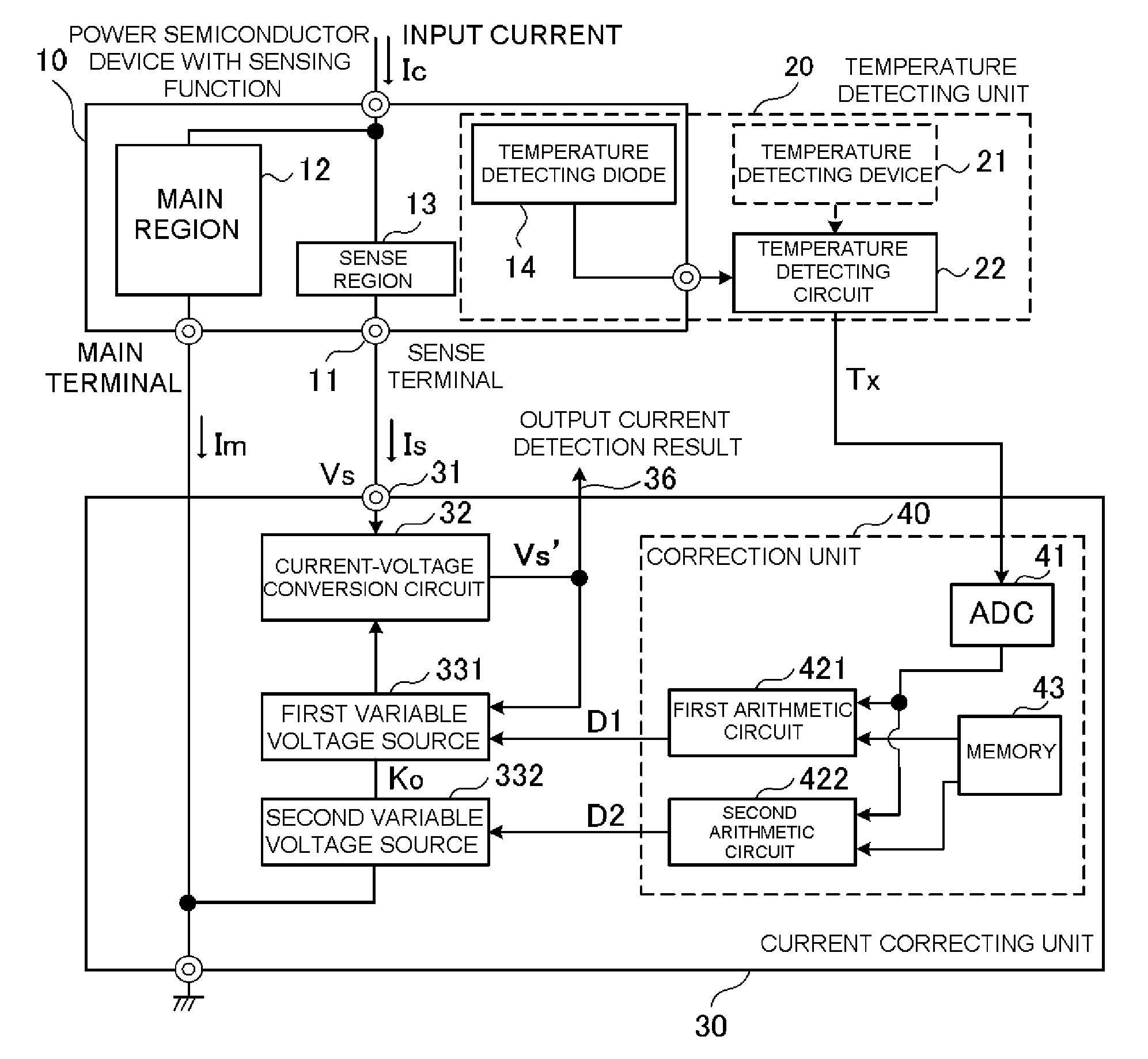
[0048]FIG. 4 is a diagram illustrating an example based on the second construction principle of the current detecting circuit for a power semiconductor device according to the embodiment of the invention. In this example, a power semiconductor device 100 is an IGBT and the IGBT has a sense terminal. When the area ratio of the sense region to the main region is 1 / W, a sense current Is which is 1 / W of the main current Im is output. A diode 114 made of, for example, polysilicon is formed on the IGBT device 100 and is used as a temperature detecting device. A detecting circuit 220 of a temperature detecting unit 200 amplifies an output from the temperature detecting diode 114 using an operational amplifier 221 and outputs the amplified voltage Vf[t] to a current correcting unit 300.

[0049]A DSP (Digital Signal Processor) is used as a correction unit 340 of the current correcting unit 300. The DSP used in this example includes a communication interface (IF) 345 which can receive data from...


PUM


Abstract

A current-voltage conversion circuit of a current correcting unit having a current detecting terminal connected to a sense terminal of a power semiconductor device converts a sense current into a voltage and detects the voltage. A temperature detecting unit detects the ambient temperature of the power semiconductor device, and a correction unit performs a predetermined operation for correcting a characteristic difference due to the temperature on the basis of the detected temperature and outputs a control signal to a variable voltage source. The variable voltage source changes an output voltage on the basis of the output control signal and adjusts the potential of the sense terminal of the power semiconductor device on the basis of the changed voltage value. In this way, the characteristic difference between a main region and a sense region of the power semiconductor device is corrected.

Description

TECHNICAL FIELD[0001]The present invention relates to a current correction circuit and a current correction method which detect a sense current flowing to a power semiconductor device, such as a diode or a transistor (bipolar transistor, a MOSFET (Metal Oxide Semiconductor-Field Effect Transistor), or an IGBT (Insulated Gate Bipolar Transistor)) and correct a characteristic difference between a main region and a sense region.BACKGROUND ART[0002]An IGBT module including an IGBT and a free wheeling diode (hereinafter, which is abbreviated to an FWD), which are power semiconductor devices, is applied to a power conversion device, such as an inverter or a DC (Direct Current) chopper circuit.[0003]In general, it is necessary to detect an output current in order to control the power conversion circuit. In general, the following two methods are mainly used to detect the output current:[0004](1) A method using a current detector, such as a current transformer or a DC-CT (Direct Current-Curr...

Claims


Application Information

Patent Timeline
Patent Type & Authority Applications(United States)
IPC IPC(8): G05F1/46
CPCH03K2217/0027G01R19/32H03K2017/0806G05F1/463H03K17/0828H03K17/14
Inventor KAWASHIMA, TETSUYA
Owner FUJI ELECTRIC CO LTD
Why Eureka
Try Eureka