

Semiconductor device
a technology of semiconductors and current sensors, applied in the field of semiconductor devices, can solve the problems of low current sensing accuracy and enlarged chip area, and achieve the effect of improving current sensing accuracy
- Summary
- Abstract
- Description
- Claims
- Application Information
AI Technical Summary
Benefits of technology
Problems solved by technology
Method used
Image

Examples
first embodiment
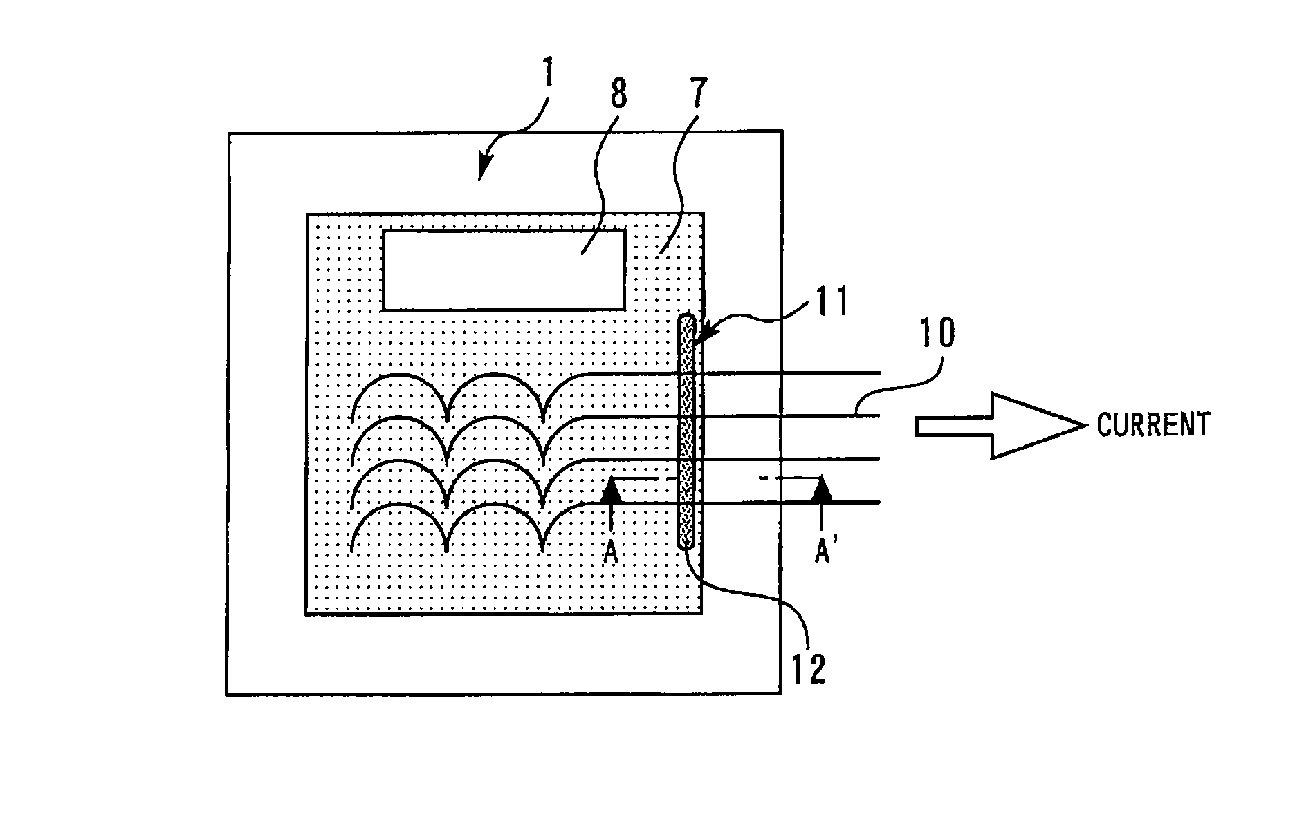
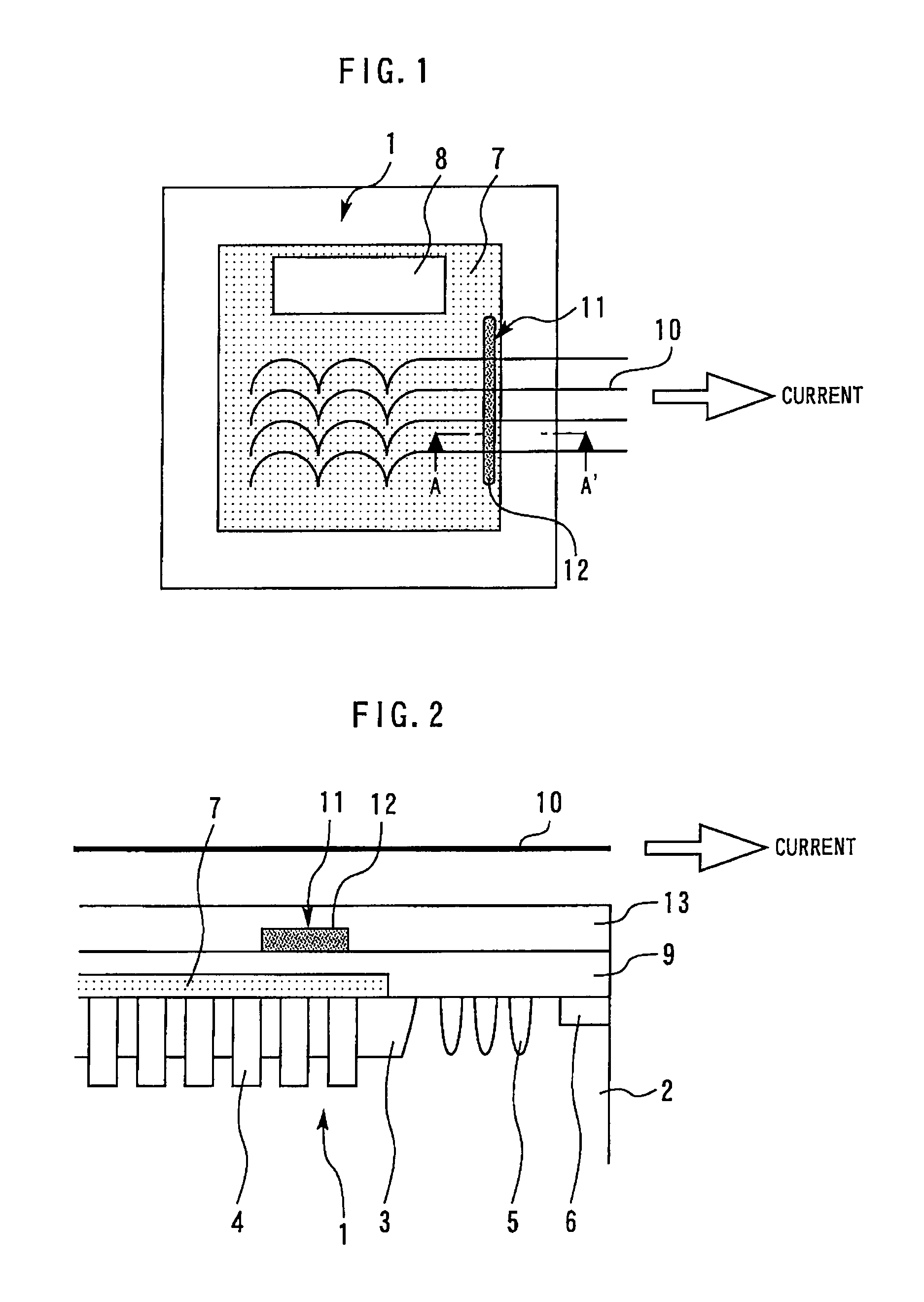
[0025]FIG. 1 is a plan view showing a semiconductor device according to the first embodiment of the present invention. FIG. 2 is a sectional view taken along the line A-A′ in FIG. 1. A semiconductor element 1 is an insulated gate bipolar transistor (IGBT) applied to a power converter, such as an inverter. A p-type well base region 3 is formed in the vicinity of the surface of a semiconductor substrate 2. Trench gates 4 are formed so as to penetrate a p-type well base region 3. Guard ring P-type well regions 5 and an N+-type channel stopper 6 are formed around the p-type well base region 3. An emitter electrode 7 and a gate electrode 8 are formed on the surface side of the chip. The emitter electrode 7 is coated with an insulating isolation film 9.
[0026]Leading lines 10 are electrically connected to the emitter electrode 7. The leading lines 10 pass above the emitter electrode 7 and are led to the side. Generally, the leading lines 10 are wires for wire bonding; however, they are not...
second embodiment
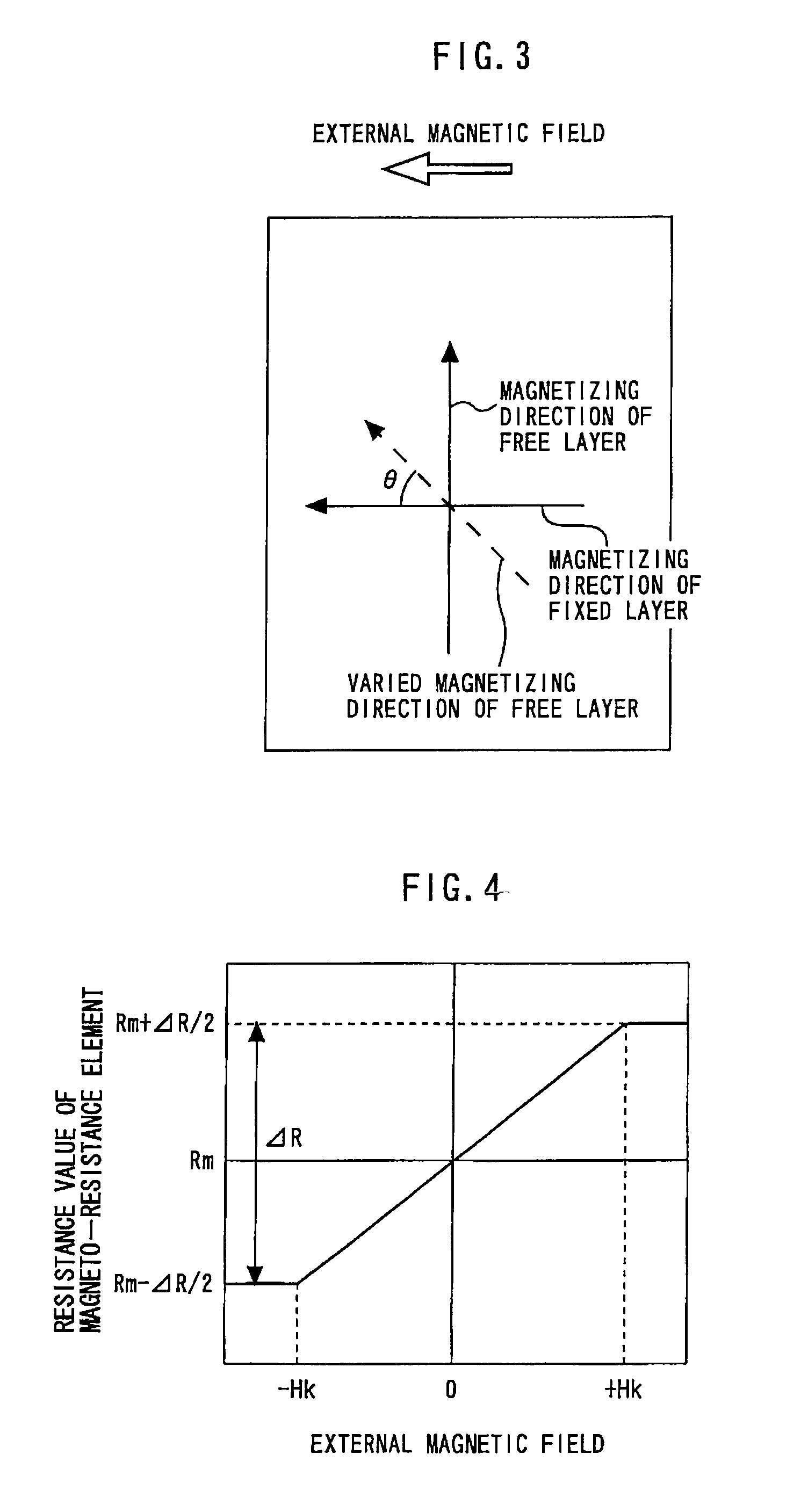
[0037]FIG. 6 is a plan view showing a semiconductor device according to the second embodiment of the present invention. The current sensor 11 further includes first and second ferromagnetic bodies 14a and 14b. The first and second ferromagnetic bodies 14a and 14b extend at right angle to the current direction, and are placed so as to pinch the magneto-resistance element 12. Thereby, since magnetic fields generated when applying a current can be converged, the sensitivity of the magneto-resistance element 12 can be improved.
third embodiment
[0038]FIG. 7 is a plan view showing a semiconductor device according to the third embodiment of the present invention. FIG. 8 is a sectional view taken along the line A-A′ in FIG. 7. A bridge-shaped body 15 composed of a ferromagnetic material is connected to the first and second ferromagnetic bodies 14a and 14b. The bridge-shaped body 15 is insulated from the magneto-resistance element 12 and the leading line 10. Since magnetic fields can be further converged by the bridge-shaped body 15, the sensitivity of the magneto-resistance element 12 can further be improved.
[0039]Alternatively, the bridge-shaped body 15 can be formed by sputtering after forming the first and second ferromagnetic bodies 14a and 14b followed by forming and patterning the insulating isolation film, or the bridge-shaped body 15 previously formed as housing can be joined to the first and second ferromagnetic bodies 14a and 14b.
PUM
 Abstract
Description
Claims
Application Information