

Semiconductor integrated circuit and method of designing thereof based on TPI
a technology of integrated circuit and semiconductor, applied in the direction of software simulation/interpretation/emulation, instruments, program control, etc., can solve the problems of increasing circuit malfunction, and the increase of the malfunction caused by the small delay defect, so as to reduce avoid unnecessary increase in the number of test points, and reduce the overlook of the small delay defect
- Summary
- Abstract
- Description
- Claims
- Application Information
AI Technical Summary
Benefits of technology
Problems solved by technology
Method used
Image

Examples
first example
2-1. First Example
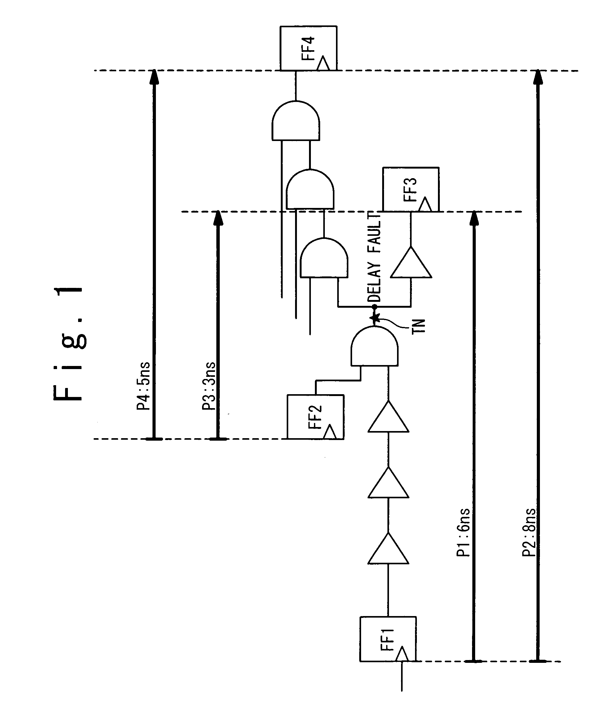
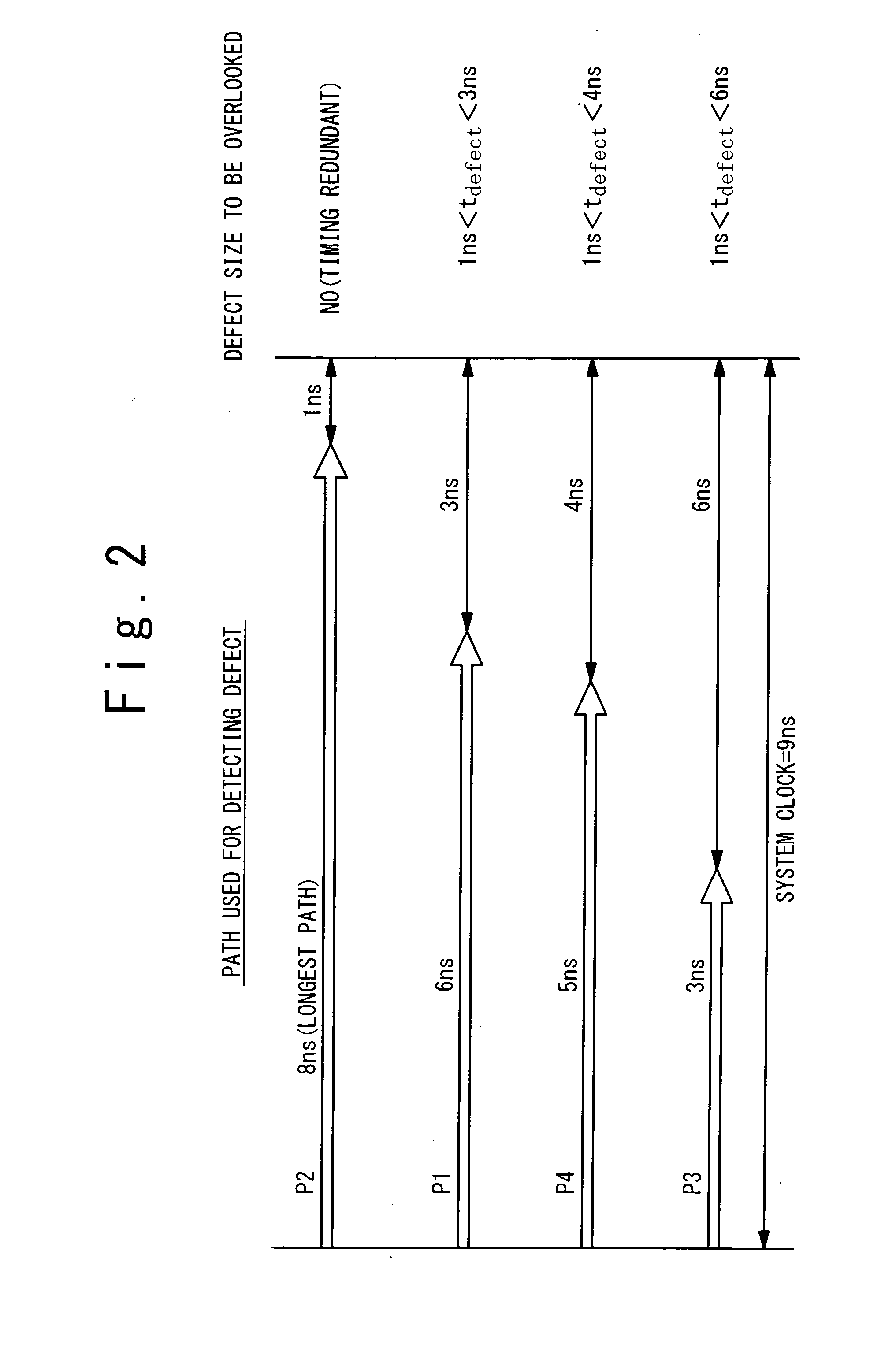
[0045]FIG. 5 shows a first example of the design circuit according to the present embodiment. The design circuit shown in FIG. 5 includes flip-flops (scan flip-flops) FF1 to FF4, as in the case shown in FIG. 1. As shown in FIG. 5, a test point TP (observation flip-flop) is inserted at a target node TN within the design circuit. A path from the flip-flop FF1 to the test point TP is the test point path PT. The longest path, whose delay time is the maximum among paths other than the test point path PT passing through the target node TN, is the path P2 (delay time: 8 ns) from the flip-flop FF1 to the flip-flop FF4.
[0046]In Step S200, a TP delay is designated with respect to the test point path PT. In the first example, the delay time (8 ns) of the longest path P2 is designated as the TP delay. In other words, the TP delay is set to be equal to the delay time of the longest path P2 that would be a preferable path used in the delay testing if the test point TP is not ins...
second example
2-2. Second Example
[0048]FIG. 6 shows a second example of the design circuit according to the present embodiment. The description overlapping with the first example will be omitted as appropriate. In the second example, a test clock cycle (test timing) at the time of the delay testing is designated as the TP delay. In the present example, the test clock cycle is 9 ns and thus the TP delay is set to 9 ns. The TP delay is the maximum among delay times of paths passing through the target node TN. In order that the designated TP delay is achieved, some inverters as delay elements are inserted as shown in FIG. 6. As a result, the test point path PT with delay time of 9 ns is obtained.
[0049]The test point path PT is used in the delay testing. Therefore, even if a small delay defect occurs at the target node TN, the small delay defect is not overlooked but detected precisely. That is, the same effect as in the first example can be obtained. Moreover, the detection accuracy of the small del...
third example
2-3. Third Example
[0051]In the foregoing examples, the cases of the observation test point have been explained. The same applies to a case of a control test point. FIG. 7 shows an example of a case where a control test point is inserted. A design circuit shown in FIG. 7 includes flip-flops (scan flip-flops) FF5 to FF8. Also, a test point TP (control flip-flop) is inserted at a target node TN. A path from the test point TP to the flip-flop FF8 is the test point path PT. A certain TP delay is designated with respect to the test point path PT. For example, the TP delay is set to be equal to a delay time of the longest path P5 passing through the target node TN. Alternatively, the TP delay may be set to be equal to the test clock cycle at the time of the delay testing.
[0052]3. Method of Determining Test Point Insertion Position
[0053]As described above, the test point TP according to the present embodiment can support detection of the small delay defect. Next, a method of determining whe...
PUM
 Abstract
Description
Claims
Application Information