Semiconductor integrated circuit device

a technology of integrated circuits and semiconductors, applied in the direction of logic circuit coupling/interface arrangement, logic circuit coupling/interface using field-effect transistors, pulse techniques, etc., can solve problems such as breakdown or destruction of hvi

Active Publication Date: 2016-10-20
FUJI ELECTRIC CO LTD
View PDF2 Cites 8 Cited by
  • Summary
  • Abstract
  • Description
  • Claims
  • Application Information

AI Technical Summary

Benefits of technology

[0055]The semiconductor integrated circuit device further includes a fourth well region of the second conductivity type, and disposed on the surface layer of the first surface of the semiconductor layer, adjacent to the third well region so that the third well is between the fourth well region and the first well region; a first circuit unit disposed in the fourth well region; a second circuit unit disposed in the first well region; and a third ci...

Problems solved by technology

This may cause malfunction or latch-up of the high-side circuit unit 217...

Method used


Image

  • Semiconductor integrated circuit device
  • Semiconductor integrated circuit device
  • Semiconductor integrated circuit device

Examples


first embodiment

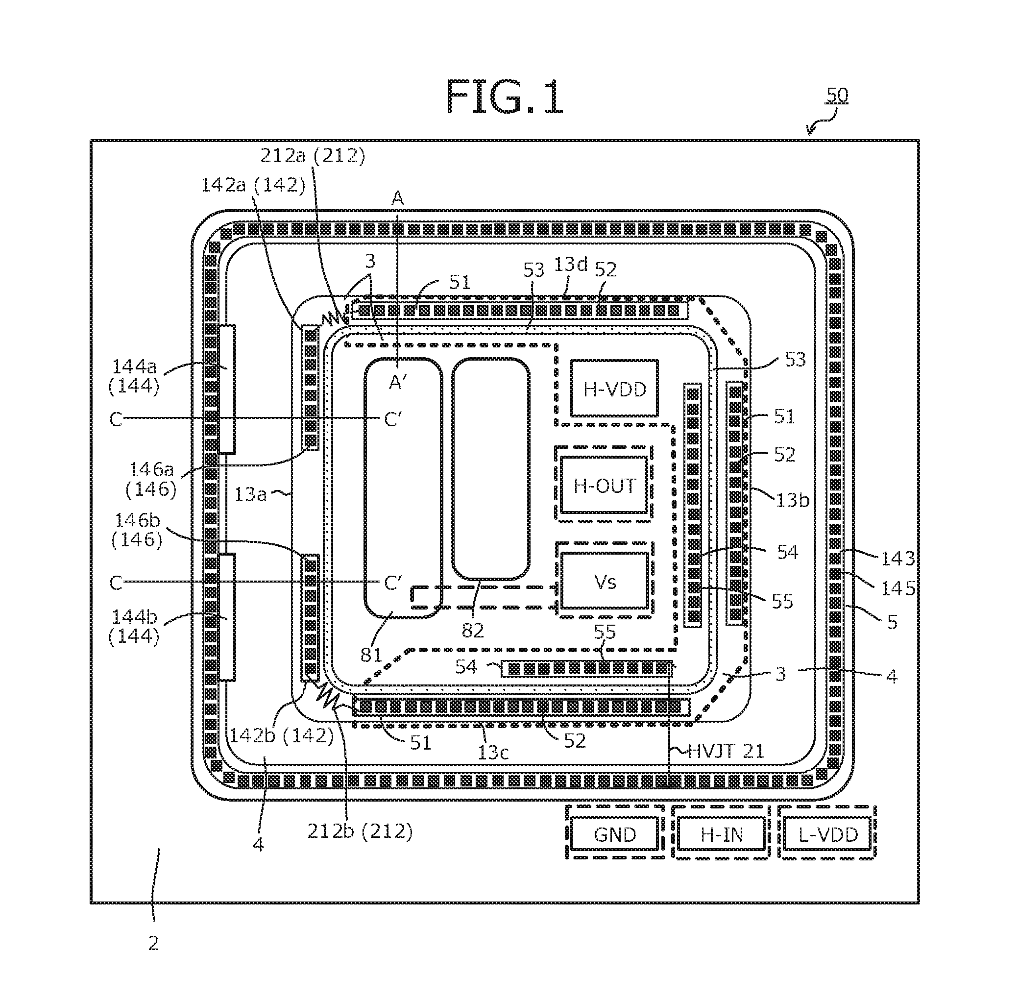
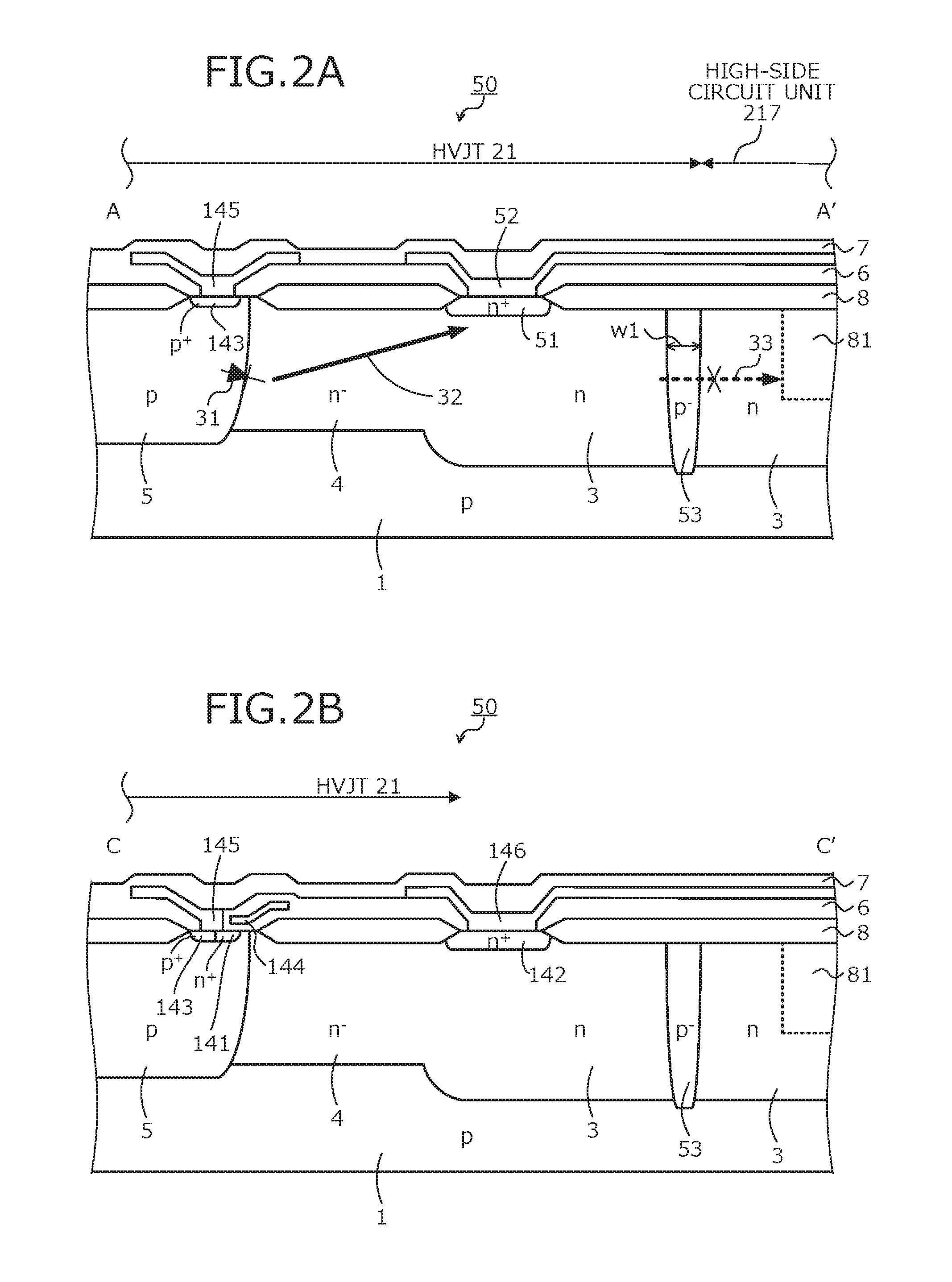
[0073]A planar layout of the HVIC 50 will first be described. As depicted in FIG. 1, the HVIC 50 includes a high-potential region, a low-potential region, and a HVJT 21 on a p-type semiconductor substrate (semiconductor layer of a first conductivity type) 1. The high-potential region is a region to which voltage at a potential of an H-VDD (a third potential) and voltage at a potential of a Vs (a second potential) of the HVIC 50 are applied. For example, the high-potential region is an n-type well region (first well region of a second conductivity type) 3 disposed on the front surface side of the p-type semiconductor substrate 1. For example, in the high-potential region, a high-side circuit unit (second circuit unit), which is a peripheral circuit of the level shifter circuit, is disposed.

[0074]The low-potential region is a region to which voltage at a potential of an L-VDD (fourth potential) and voltage at a GND (first potential) of the HVIC 50 are applied. For example, the low-po...

second embodiment

[0116]Alternately, the second embodiment may be applied such that the dielectric region 73 is disposed between the n-type well region 3 and the n−-type well region 4 so as to contact the n-type well region 3 and the n−-type well region 4. The trench 71 may be formed to penetrate the n−-type well region 4 from the substrate front surface to the remaining portion of the p-type semiconductor substrate 1 and the dielectric material film 72 may be embedded such that the dielectric region 73 is interposed between the n−-type well regions 4 located on the chip center side and the chip perimeter side.

[0117]Even when the fourth embodiment is applied to the second or third embodiment described above such that the dielectric region 73 is disposed instead of the p−-type isolation region, effects identical to those of the fourth embodiment are achieved.

[0118]As described above, the fourth embodiment achieves effects identical to those of the first to third embodiments.

[0119]A structure of a semi...

fifth embodiment

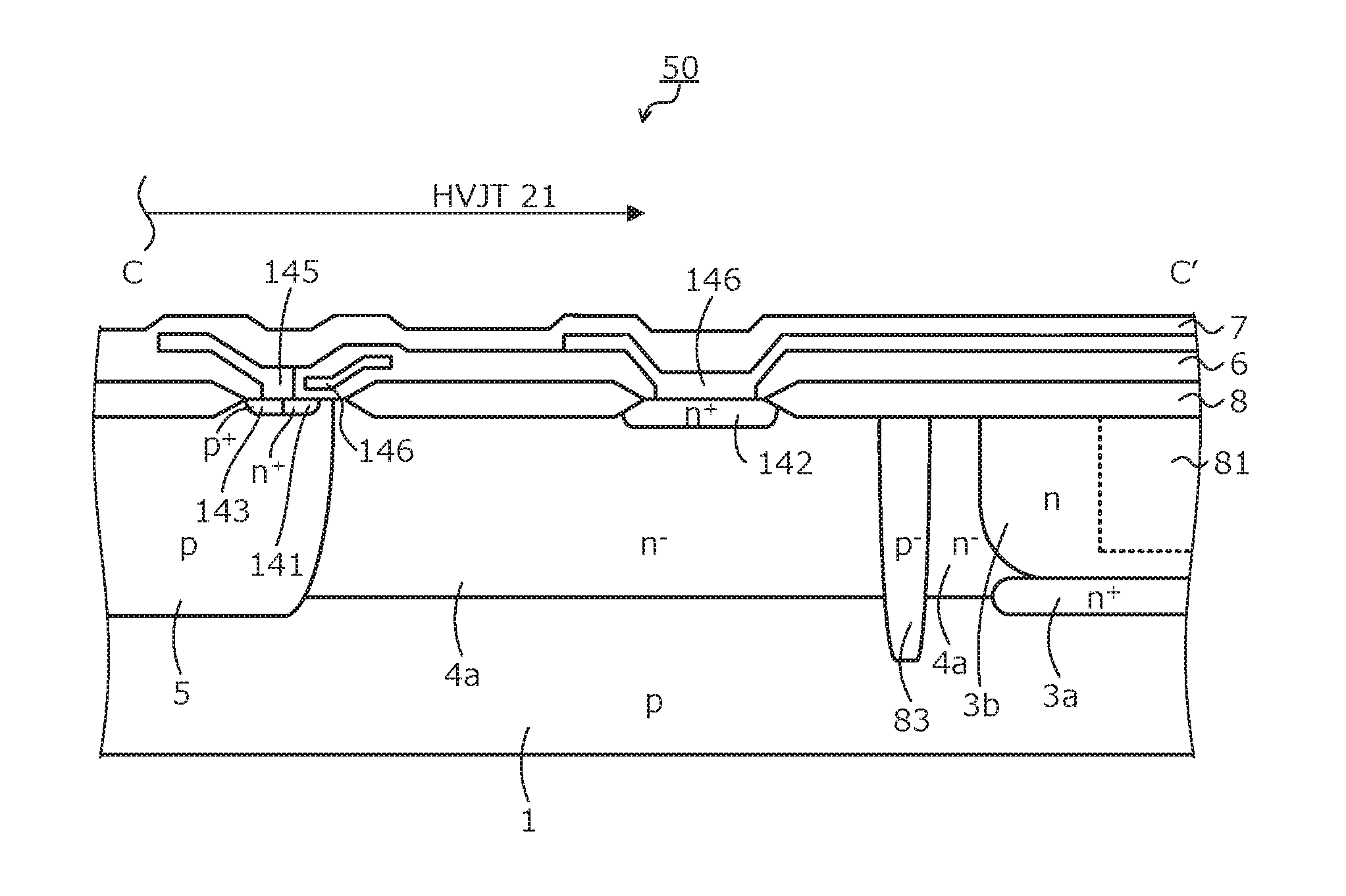
[0120]FIGS. 9A and 9B are cross-sectional views of a main portion of a high-voltage integrated circuit device according to the In an example of an embedded epitaxial growth substrate of FIGS. 9A and 9B, after introducing into the surface of the p-type semiconductor substrate 1, impurities for forming an n+-type embedded layer 3a, an epitaxial layer 4a is stacked on the p-type semiconductor substrate 1, and an n-type well region 3b formed by a layer diffused from the surface of the epitaxial layer 4a is formed on the n+-type embedded layer 3a. A p−-type isolation region 83 is made of a diffusion layer extending from the surface of the epitaxial layer 4a to the p-type semiconductor substrate 1.

[0121]Even when the fifth embodiment is applied to the second or fourth embodiment described above to use the epitaxial substrate or the embedded epitaxial substrate, effects identical to those of the fifth embodiment are achieved.

[0122]As described, the fifth embodiment achieves effects identi...


PUM


Abstract

A semiconductor integrated circuit device, including a semiconductor layer of a first conductivity type, a first well region of a second conductivity type, a second well region of the second conductivity type, and a third well region of the first conductivity type. The device further includes an isolation region electrically isolating a predetermined region in the first well region, a first high-concentration region of the second conductivity type, disposed outside the isolation region and inside one of the first well region and the second well region, and a second high-concentration region of the second conductivity type, disposed inside the isolation region and inside one of the first well region and the second well region. The first and second high-concentration regions each have an impurity concentration that is higher than that of the first well region.

Description

CROSS REFERENCE TO RELATED APPLICATIONS[0001]This is a continuation application of International Application PCT / JP2015 / 067370 filed on Jun. 16, 2015, which claims priority from a Japanese Patent Application No. 2014-137241 filed on Jul. 2, 2014. The contents of the applications are incorporated herein by reference.BACKGROUND OF THE INVENTION[0002]1. Field of the Invention[0003]The embodiments discussed herein are related to a semiconductor integrated circuit device.[0004]2. Description of the Related Art[0005]High-voltage integrated circuit devices (HVICs) of an element isolation system utilizing high-voltage junction are semiconductor integrated circuit devices that drive and turn on / off switching power devices making up an upper arm of a bridge circuit for power inversion (DC-AC conversion) such as a pulse width modulation (PWM) inverter. An HVIC has a means of detecting overcurrent and temperature during times of malfunction of the switching power device and thereby affords high...

Claims


Application Information

Patent Timeline
IPC IPC(8): H03K19/0185H03K17/567H01L29/739H01L29/10H01L27/082H01L29/06
CPCH03K19/018521H01L27/082H03K17/567H01L29/7393H01L29/1095H01L29/0649H02M7/003H01L21/823892H01L27/092H01L27/0922H01L29/861H01L21/76224H01L21/761H01L21/76
Inventor YAMAJI, MASAHARU
Owner FUJI ELECTRIC CO LTD
Why Eureka
Try Eureka