Semiconductor integrated circuit and method of designing semiconductor integrated circuit

a technology of integrated circuits and semiconductors, applied in logic circuits using specific components, pulse techniques, instruments, etc., can solve the problems of reducing the withstanding voltage, time dependent dielectric breakdown (tddb) when a voltage is applied, and unfavorable factor for increasing the chip area, so as to prevent the tddb from deteriorating

Active Publication Date: 2007-09-06
SOCIONEXT INC
View PDF9 Cites 8 Cited by
  • Summary
  • Abstract
  • Description
  • Claims
  • Application Information

AI Technical Summary

Benefits of technology

[0012]Therefore, a main object of the present invention is to make prevention of TDDB deterioration prevent possible in as many cells as possible while controlling increase of a chip area.

Problems solved by technology

However, thinning of the gate oxide film leads to reduction of a withstanding voltage of the gate oxide film and may cause the time dependent dielectric breakdown (TDDB) when a voltage is applied.
As a result, it becomes necessary to add the TDDB control circuit individually in each of the cells where prevention of the TDDB deterioration is requested, which is an unfavorable factor for increase of a chip area.

Method used


Image

  • Semiconductor integrated circuit and method of designing semiconductor integrated circuit
  • Semiconductor integrated circuit and method of designing semiconductor integrated circuit
  • Semiconductor integrated circuit and method of designing semiconductor integrated circuit

Examples


embodiment 1

Preferred Embodiment 1

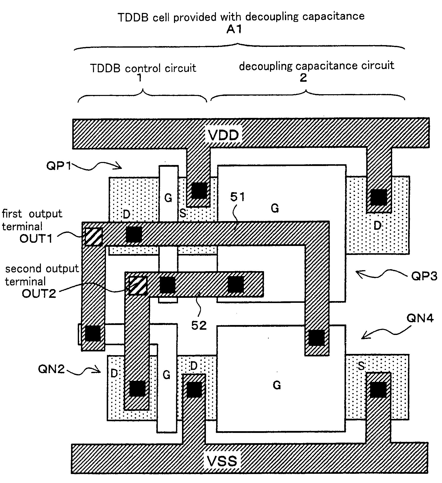
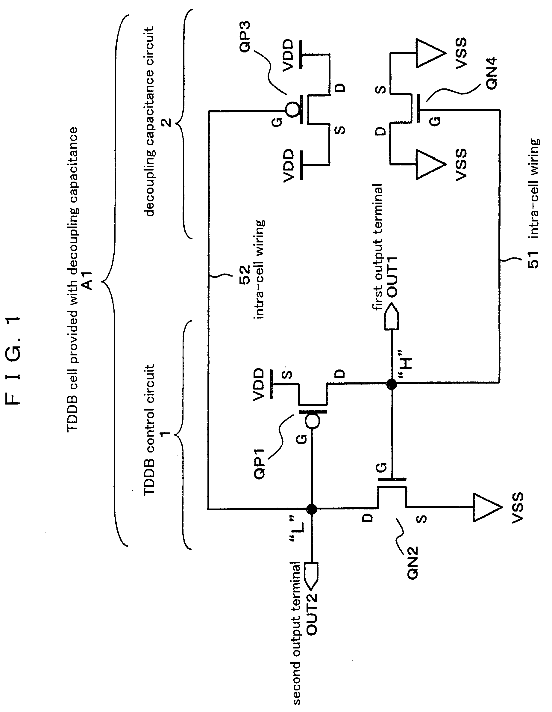
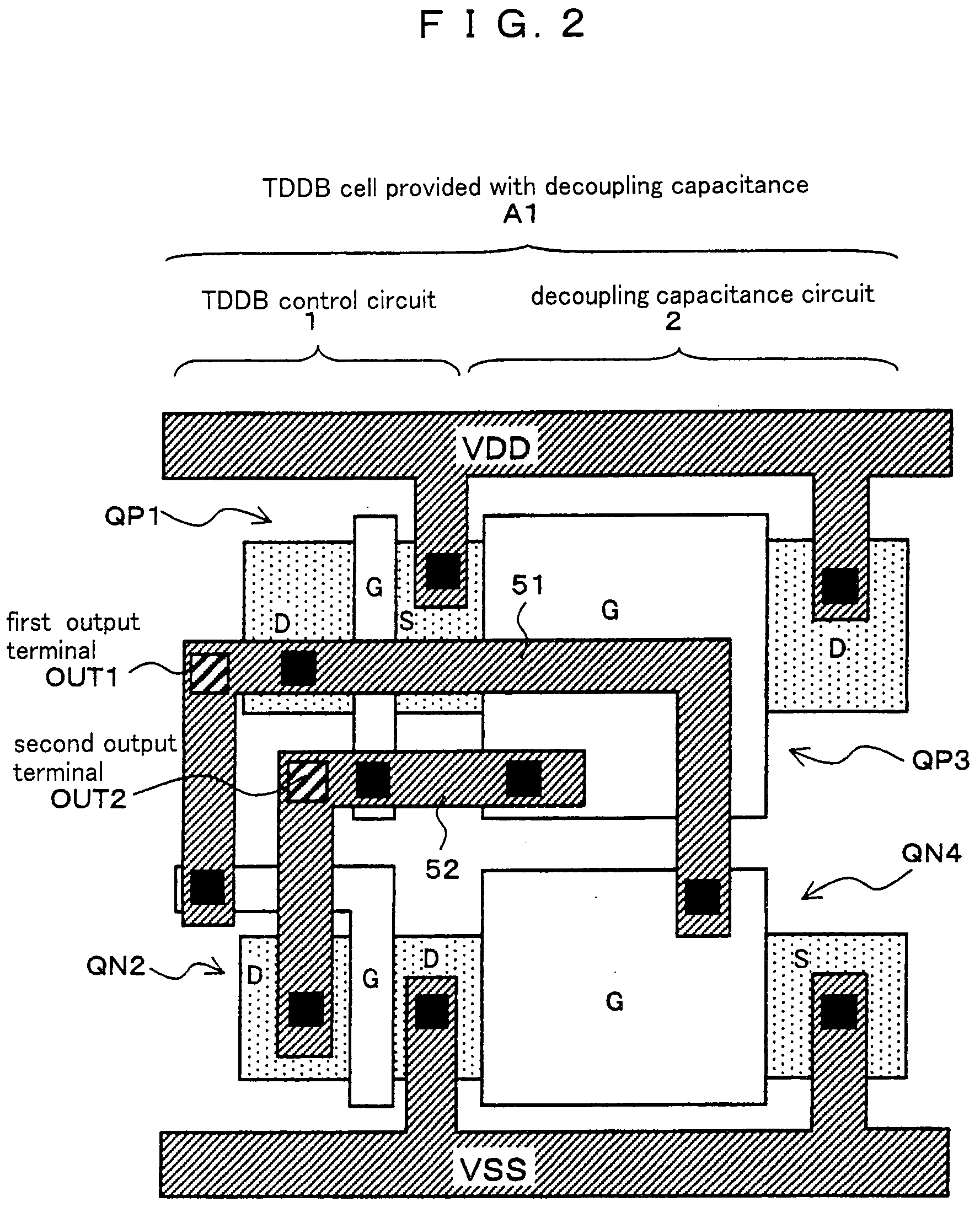
[0106]FIG. 1 is a circuit diagram illustrating a TDDB control cell A1 provided with a decoupling capacitance as a semiconductor integrated circuit according to a preferred embodiment 1 of the present invention. FIG. 2 is a layout plan view of the TDDB control cell A1. The TDDB control cell A1 comprises a TDDB control circuit 1 and a decoupling capacitance circuit 2 connected to the TDDB control circuit 1.

[0107]The TDDB control circuit 1 includes a first transistor QP1 of P-channel type and a second transistor QN2 of N-channel type. A source of the first transistor QP1 is connected to a high-voltage power supply wiring (VDD). A source of the second transistor QN2 is connected to a low-voltage power supply wiring (VSS). A gate of the first transistor QP1 is connected to a drain of the second transistor QN2. A drain of the first transistor QP1 is connected to a gate of the second transistor QN2.

[0108]The decoupling capacitance circuit 2 comprises a third transisto...

embodiment 2

Preferred Embodiment 2

[0123]FIG. 5 is a circuit diagram illustrating a TDDB control cell A2 provided with a correction circuit as a semiconductor integrated circuit according to a preferred embodiment 2 of the present invention. FIG. 6 is a layout plan view of the TDDB control cell A2.

[0124]The TDDB control cell A2 provided with the correction circuit according to the present preferred embodiment comprises a TDDB control circuit 1 and a correction circuit 3. The TDDB control circuit 1 is constituted in a manner similar to the preferred embodiment 1 and is not described again. The correction circuit 3 is a cell having the same role as that of the correction cells 20, 21 and 22 shown in FIG. 3 according to the preferred embodiment 1. An inverter comprising a fifth transistor QP5 of the P-channel type and a sixth transistor QN6 of the N-channel type, can be quoted as a constitutional example of the correction circuit 3. A source of the fifth transistor QP5 is connected to a high-voltag...

embodiment 3

Preferred Embodiment 3

[0126]FIG. 7 is a circuit diagram illustrating a decoupling capacitance cell A3 as a semiconductor integrated circuit according to a preferred embodiment 3 of the present invention. FIG. 8 is a layout plan view of the decoupling capacitance cell A3. The decoupling capacitance cell A3 comprises a transistor QP7 of the P-channel type and an eighth transistor QN8 of the N-channel type. A drain and a source of the transistor QP7 of the P-channel type are connected to a high-voltage power supply wiring (VDD). A drain and a source of the transistor QN8 of the N-channel type are connected to a low-voltage power supply wiring (VSS). An input terminal IN7 is connected to a gate of the transistor QP7 of the P-channel type. An input terminal IN8 is connected to a gate of the transistor QN8 of the N-channel type.

[0127]FIG. 9 is a layout plan view illustrating a part of a logical block including decoupling capacitance cells A3 and A3′ and the TDDB control cell A1 provided w...


PUM


Abstract

In the present invention, a decoupling capacitance circuit, a first output terminal and a second output terminal are provided. The decoupling capacitance circuit comprises a TDDB control circuit consisting of a first Tr and a second Tr, and a third Tr. Conductivity types of the first and second Trs are different from each other. A source of the first Tr is connected to a first power supply wiring, and a drain of the first Tr is connected to a gate of the second Tr. A source of the second Tr is connected to a second power supply wiring, and a drain of the second Tr is connected to a gate of the first Tr. The third and first Trs have the same conductivity type. A source and a drain of the third Tr are connected to the first power supply wiring, and a gate of the third Tr is connected to the drain of the second Tr. The first output terminal is connected to the drain of the first Tr, and the second output terminal is connected to the drain of the second Tr.

Description

BACKGROUND OF THE INVENTION[0001]1. Field of the Invention[0002]The present invention relates to a semiconductor integrated circuit and a method of designing the semiconductor integrated circuit for a purpose of protecting a gate oxide film of a transistor.[0003]2. Description of the Related Art[0004]In recent years, miniaturization of constituent elements in a semiconductor integrated circuit has been largely advanced. Above all, film thinning has been remarkably progressed in a gate oxide film in an MOS (Metal Oxide Semiconductor) transistor. However, thinning of the gate oxide film leads to reduction of a withstanding voltage of the gate oxide film and may cause the time dependent dielectric breakdown (TDDB) when a voltage is applied. Therefore, caution for the time dependent dielectric breakdown (TDDB) should be needed with respect to a circuit where a power supply voltage is constantly applied to a gate. Examples of such a circuit are a decoupling capacitance cell, a correction...

Claims


Application Information

Patent Timeline
Patent Type & Authority Applications(United States)
IPC IPC(8): H01L29/94
CPCH01L27/11807H01L27/0203
Inventor MIZUSHINO, EMINISHIMURA, HIDETOSHIYANO, JUNICHI
Owner SOCIONEXT INC
Why Eureka
Try Eureka