Nonvolatile semiconductor memory device and its writing method

a non-volatile semiconductor and memory device technology, applied in static storage, digital storage, instruments, etc., can solve the problems of gradual deviation of threshold voltage once written and set, and worsening of read-out margins, so as to prevent the distribution of threshold voltage

Inactive Publication Date: 2007-05-31
SHARP KK
View PDF6 Cites 8 Cited by
  • Summary
  • Abstract
  • Description
  • Claims
  • Application Information

AI Technical Summary

Benefits of technology

[0026] This could not only make it possible to prevent threshold voltage distribution from being diffused due to effects of adjacent memory cells, first by using the first external write command and writing data into all memory cells to be affected by capacitive coupling from adjacent memory cells, and then by using the second external write command and writing the same data as that written by using the first external write command to the same address to which writing is performed by using the first external write command, but also eliminate the need for retaining in the nonvolatile memory much data to be written since an external writing system such as PROM writer, for example, can be used by using respective external commands when writing data, thereby enabling control of increased chip area.

Problems solved by technology

However, in line with reduction of memory cell size due to the miniaturization trend in recent years, as data is often written into one memory cell, and then into memory cells adjacent to that memory cell, a risk that threshold voltage that has been once written and set will suffer from a deviation due to effects of the adjacent memory cells, and thereby read-out margins gradually will worsen has been pointed out.
Then, readout margin worsens, and readout error may occur in the worst case.
Thus, the threshold voltage of the cell when writing is performed into the adjacent memory cells will further increase and worsen the readout margin, thus causing a major obstacle of miniaturization.
However, there exist two problems in the technology of the known publication.
The first problem is that effects of memory cells on adjacent word lines cannot be alleviated, while effects of memory cells on adjacent bit lines can be eliminated.
The second problem is that in order to perform writing as described in the known publication, writing data of when pre-writing is done to the even columns should be continuously retained in a latch circuit even when post-writing is done to the odd columns.
As the number of columns increases, latch circuits will also be needed accordingly, thus leading to expansion of chip area.

Method used


Image

  • Nonvolatile semiconductor memory device and its writing method
  • Nonvolatile semiconductor memory device and its writing method
  • Nonvolatile semiconductor memory device and its writing method

Examples


Embodiment Construction

[0047] In the following, we describe embodiments of a nonvolatile semiconductor memory device according to the present invention and a method of writing thereto (hereinafter abbreviated as “a device of the present invention” and “a method of the present invention”, as appropriate), based on the drawings.

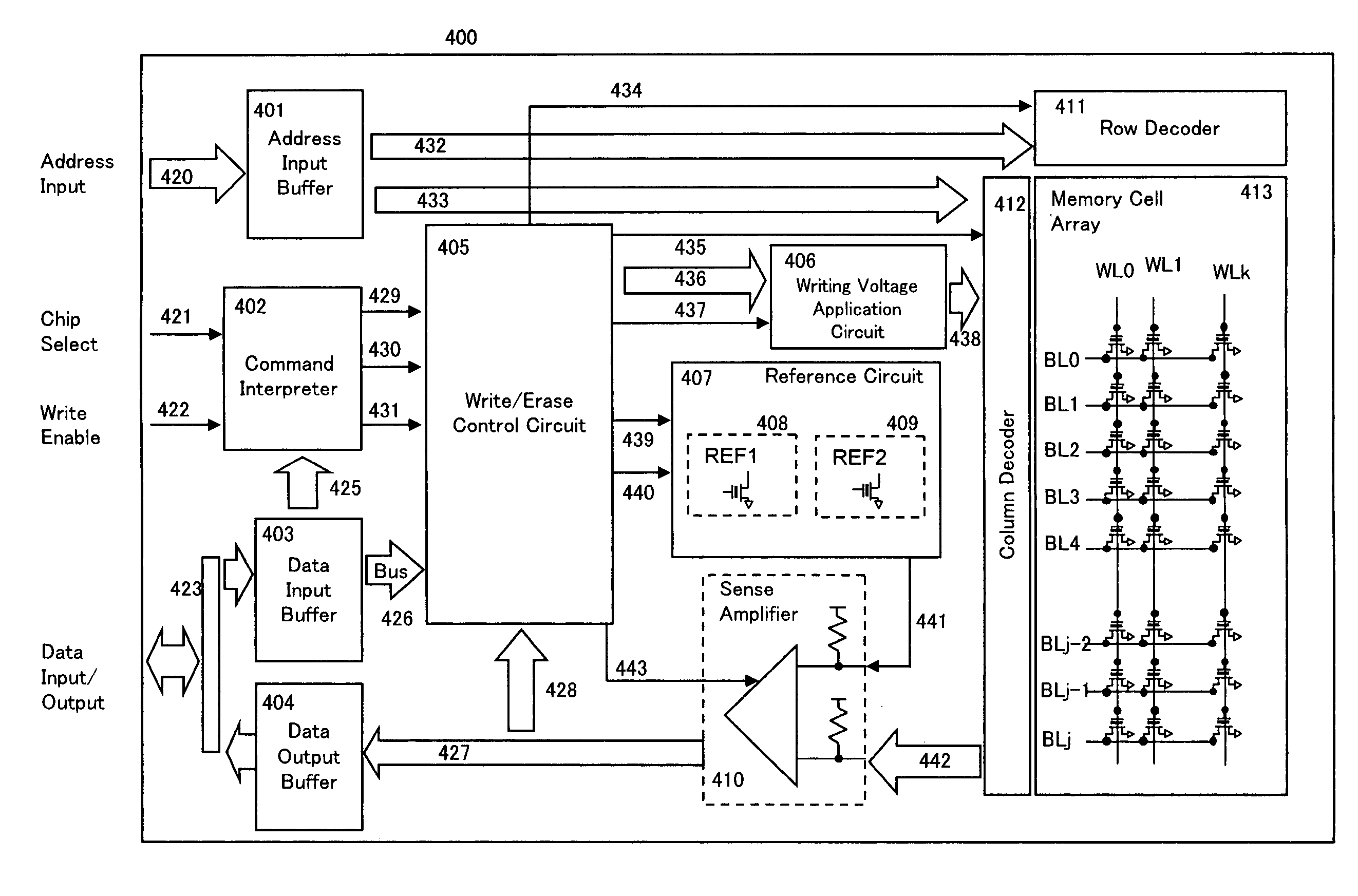
[0048]FIG. 1 is a circuit block diagram of one embodiment of a device of this invention 400. In this embodiment, it comprises memory cell arrays consisting of memory cells comprising nonvolatile transistors capable of electrically writing, erasing and reading out information arranged in a matrix in a row direction and in a column direction. As nonvolatile transistors comprising the memory cells, a floating gate type MOS transistor that has a floating gate, and is configured to perform writing by injecting channel hot electrons and erasing by using Fowler-Nordheim current (FN current) is used. In the memory cell array 413, bit lines BL0 to BLj and word lines WL0 to WLk are arranged, ...


PUM


Abstract

There is provided a nonvolatile semiconductor memory device and its writing method capable of controlling an increase in threshold voltage due to effects of adjacent memory cells and performing stable readout operations even if miniaturization of semiconductor memory devices proceeds further. The device comprises a memory cell array 411 having memory cells in a row and column directions, a row selection circuit 412, a column selection circuit 411, and a control circuit 405 for exercising writing control on a selected memory cell by an external command input. The control circuit performs a threshold voltage control for writing a memory cell selected as a writing target to a first predetermined threshold voltage when receiving a first external write command, and performs another threshold voltage control for writing the selected memory cell to a second predetermined threshold voltage different from the first threshold voltage when receiving a second external write command.

Description

CROSS REFERENCE TO RELATED APPLICATION [0001] This Nonprovisional application claims priority under 35 U.S.C. § 119(a) on patent application No. 2005-345638 filed in Japan on 30 Nov., 2005, the entire contents of which are hereby incorporated by reference. BACKGROUND OF THE INVENTION [0002] 1. Field of the Invention [0003] The present invention relates to a semiconductor memory device and specifically to a nonvolatile semiconductor memory device and a method of writing data thereto. [0004] 2. Description of the Related Art [0005] As a nonvolatile semiconductor memory device (hereinafter referred to a nonvolatile memory) represented by a flash memory does not lose saved data even when the power is turned off, it is widely used in all products ranging from digital mobile devices such as a cellular phone, digital camera, portable music player, etc., to networking equipment such as a digital TV, set top box, or a router, etc., and is expected to find widespread applications in the futur...

Claims


Application Information

Patent Timeline
Patent Type & Authority Applications(United States)
IPC IPC(8): G11C7/00
CPCG11C16/12G11C16/28G11C16/3459G11C16/0483G11C16/30
Inventor NAWAKI, MASARU
Owner SHARP KK
Why Eureka
Try Eureka