Two-step sub-ranging analog-to-digital converter and method for performing two-step sub-ranging in an analog-to-digital converter

a technology of analog-to-digital converter and two-step sub-ranging, which is applied in the field of two-step sub-ranging adc, can solve the problems of large area, large amount of power consumed by flash adc, and the need for comparators to be extremely fast, so as to increase the overall timing margin window without increasing power consumption and without increasing the amount of die area required

Inactive Publication Date: 2010-04-29
BROADCOM INT PTE LTD
View PDF4 Cites 7 Cited by
  • Summary
  • Abstract
  • Description
  • Claims
  • Application Information

AI Technical Summary

Benefits of technology

[0011]The invention is directed to a two-step sub-ranging ADC and method that provide an increased overall timing margin window without increasing power consumption and without increasing the amount of die area required for implementation of the ADC. The ADC comprises a first sampler/buffer circuit, a second sampler/buffer circuit, a first MUX, a second MUX, a CADC circuit, an FADC circuit, a sub-ranging MUX, and an encoder. The first sampler/buffer circuit is configured to obtain odd samples of an analog input signal, ADC_IN, during odd phases of a first clock signal, ADC_CLK. The second sampler/buffer circuit is configured to obtain even samples of ADC_IN during even phases of ADC_CLK. The first MUX is configured to select an odd sample obtained by the first sampler/buffer circuit at a first in

Problems solved by technology

In order to obtain high bit resolution at high speed, however, the comparators must be extremely fast.
The use of such a large number of comparators results in a large amount of area and a large amount of power being consumed by the flash ADC.
In addition, paralleling the large number of comparators results in high input capacitance, which limits the overall conversion speed of the full flash ADC.
Consequently, two-step ADCs typically consume less power and require less chip area than full flash ADCs.
In general, the disadvantage of two-step ADCs compared to full flash ADCs is the need for a clocking scheme in two-step

Method used


Image

  • Two-step sub-ranging analog-to-digital converter and method for performing two-step sub-ranging in an analog-to-digital converter
  • Two-step sub-ranging analog-to-digital converter and method for performing two-step sub-ranging in an analog-to-digital converter
  • Two-step sub-ranging analog-to-digital converter and method for performing two-step sub-ranging in an analog-to-digital converter

Examples


Embodiment Construction

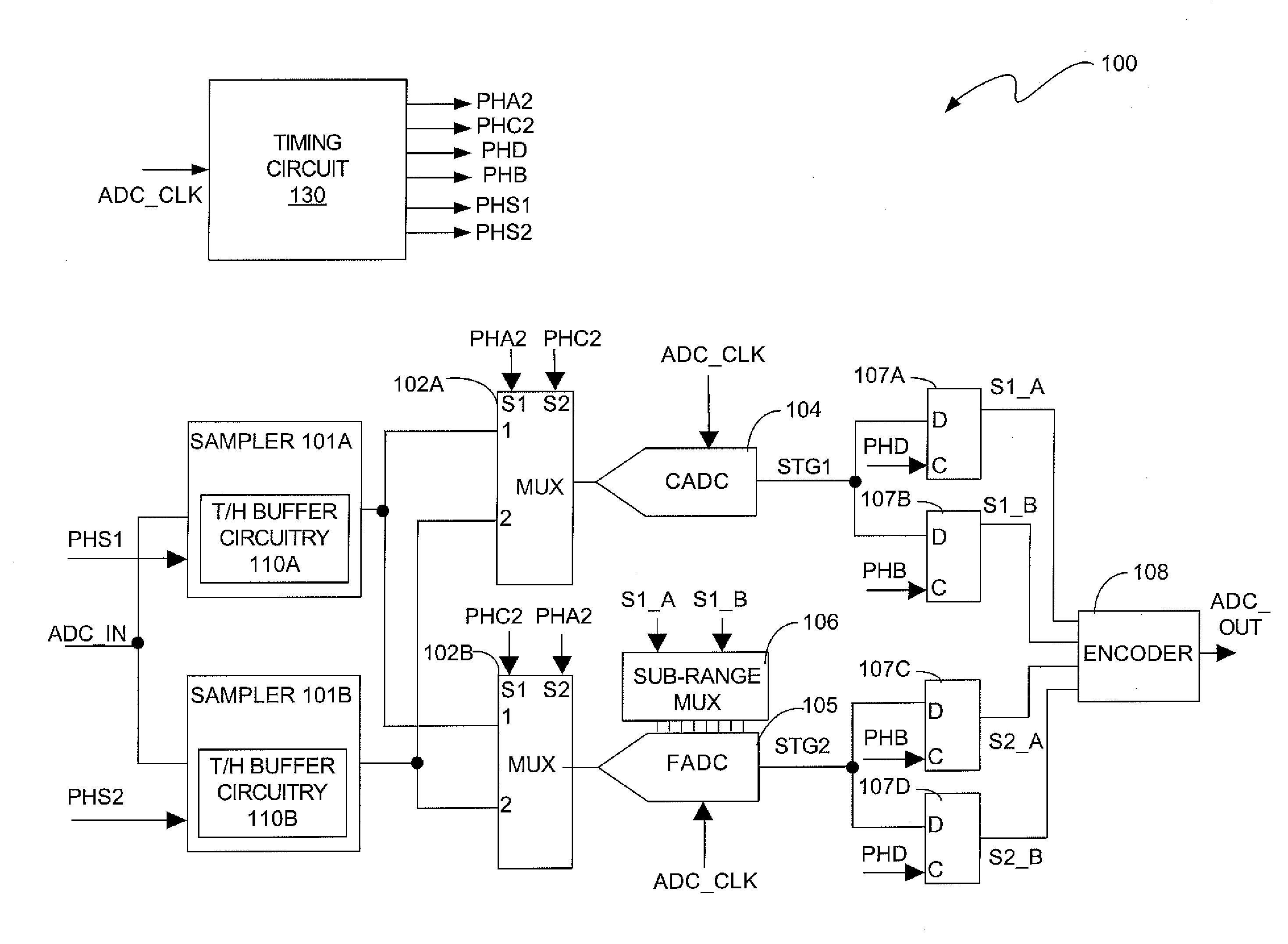
[0022]In accordance with the invention, a two-step sub-ranging ADC is provided that achieves significant improvements in the settling time window available for the CADC, MUX sub-ranging and FADC conversion processes without increasing the amount of chip area or power that are consumed by the ADC. The ADC uses interleaved sampler / buffer circuits to sample the incoming analog signal on different phases of the clock signal. MUXes provide the samples obtained by the sampler / buffer circuits to the CADC and FADC circuits in ping pong fashion in such a way that the CADC and FADC circuits are converting during every clock period. In addition, these improvements are achieved without increasing the number of potential sources of bit decision mismatches in the two-step ADC.

[0023]The two-step sub-ranging ADC is typically integrated into an integrated circuit (IC). The IC that incorporates the ADC typically also contains other types of circuits for performing other types of functions. The invent...


PUM


Abstract

A two-step ADC is provided that achieves significant improvements in the settling time window available for CDAC conversion, FADC sub-ranging and FADC conversion without increasing the amount of chip area or power that are consumed by the ADC. The ADC uses interleaved sampler/buffer circuits to sample the incoming analog signal on different phases of the clock signal. MUXes provide the samples obtained by the sampler/buffer circuits to the CADC and FADC circuits in ping pong fashion in such a way that the CADC and FADC circuits are converting during every clock period. In addition, these improvements are achieved without increasing the number of potential sources of bit decision mismatches in the two-step sub-ranging ADC.

Description

TECHNICAL FIELD OF THE INVENTION[0001]The invention relates to analog-to-digital converters (ADCs), and more particularly, to a two-step sub-ranging ADC.BACKGROUND OF THE INVENTION[0002]ADCs are used in a variety of electrical systems to convert electrical analog signals 3 into electrical digital signals. One type of ADC that is often used in electrical systems is called a full flash ADC. Another type of ADC that is often used in electrical systems is called a two-step ADC. In a full flash ADC, many comparators arranged in parallel with one another simultaneously receive the input analog voltage signal and the same clock signal. All bit decisions are made simultaneously based on the outputs of the comparators. In order to obtain high bit resolution at high speed, however, the comparators must be extremely fast. The use of such a large number of comparators results in a large amount of area and a large amount of power being consumed by the flash ADC. In addition, paralleling the larg...

Claims


Application Information

Patent Timeline
IPC IPC(8): H03M1/12
CPCH03M1/1215H03M1/361H03M1/146H03M1/122
Inventor ZHUANG, ZAILONG
Owner BROADCOM INT PTE LTD
Why Eureka
Try Eureka