Optical device, image-capturing apparatus, electronic apparatus, and method for producing optical device

a technology of optical devices and electronic equipment, applied in the direction of radio frequency controlled devices, instruments, television systems, etc., can solve the problems of forming antireflection films with defects, affecting the quality of optical devices, and requiring a lot of time and labor to form films, etc., to achieve easy adjustment, low cost, and less defects. the effect of defects

Inactive Publication Date: 2013-10-10
SEIKO EPSON CORP
View PDF6 Cites 11 Cited by
  • Summary
  • Abstract
  • Description
  • Claims
  • Application Information

AI Technical Summary

Benefits of technology

[0013]An advantage of some aspects of the invention is to provide an optical device in which a high-quality antireflection layer can be easily formed on a hard coat layer made of an inorganic material, an image-capturing apparatus, an electronic apparatus, and a method for producing an optical device.
[0017]Accordingly, since an organic material is used instead of an inorganic material as the organic antireflection layer in this application example, it is not necessary to use a vacuum vapor deposition method for forming a film. Therefore, a factor causing the adhesion of dirt, dust, etc. to a principal surface of the hard coat layer during film formation is significantly decreased, and thus, the film formation can be reliably performed and the occurrence of a defect in the antireflection film can be prevented. Further, since the contact angle of an organic antireflection layer is larger than that of an antireflection layer made of an inorganic material, after film formation, the adhesion of dirt, dust, etc. to the organic antireflection layer is less likely to occur, and therefore, the dust-proof performance can be enhanced. Further, the organic antireflection layer is composed of an organic material and does not contain a mixed oxide film of titanium and lanthanum, and therefore, uranium (U) or thorium (Th), each of which is a radioactive element, is not contained in the material as impurities, and thus, there are no adverse effects of radiation (α ray) emitted from such an element on an electronic apparatus such as an image-capturing apparatus which is disposed near the optical device.Application Example 2
[0021]According to this application example having such a configuration, in consideration of the wavelength range of a light to be used in each of various electronic apparatuses such as a pickup apparatus, a liquid crystal projector, and a camera, the thickness of the organic antireflection layer is set to an appropriate value. Accordingly, the antireflection effect of the optical device to be used in each apparatus can be increased.Application Example 4
[0029]According to this application example having such a configuration, the organic antireflection layer is formed on the light-transmissive base material by a dip-coating method in which the light-transmissive base material having the hard coat layer formed thereon is dipped in the solution, and therefore, the control or the like of the film-forming operation becomes simpler than in the case of using a vacuum vapor deposition method for forming an inorganic antireflection layer, and as a result, an optical device with less defects can be produced at low cost.Application Example 8
[0031]According to this application example having such a configuration, the organic antireflection layer is formed on the hard coat layer by a spin-coating method in which the solution is applied dropwise to the hard coat layer unified with the light-transmissive base material and rotating the base material, and therefore, in the same manner as in the case of using a dip-coating method, an optical device with less defects can be produced easily at low cost, and also the thickness of the organic antireflection layer can be more easily adjusted than in the case of using a dip-coating method.

Problems solved by technology

In the related art disclosed in PTL 1, such a series of complicated and troublesome steps are required, and therefore there is a problem that operational control items are increased, it takes a lot of time and labor to form a film, and as a result, the production cost is increased.
Moreover, there is also a problem that due to particles, dirt, dust, etc. generated during the operations from setting a base material on a jig to vacuuming in a vapor deposition apparatus, a disadvantage that an antireflection film with a defect is formed is caused.
Further, there is also a problem that in the case of using a mixed oxide film obtained by mixing titanium and lanthanum as a material of the antireflection film or the like, uranium (U) or thorium (Th), each of which is a radioactive element, may be sometimes incorporated in the mixed oxide film as impurities, and therefore, due to radiation (α ray) emitted from such an element, a defect occurs in a light-receiving section of an image-capturing device, or other disadvantage is caused.
Still further, there is a disadvantage that after film formation, dirt or dust adheres to a silicon oxide film constituting the antireflection film, for example, disposed as the outermost layer, and therefore there is a problem that a high quality cannot be maintained.
The related art disclosed in PTL 2 aims at improving spectroscopic properties, and does not solve the above-described disadvantages caused in the related art in PTL 1.

Method used


Image

  • Optical device, image-capturing apparatus, electronic apparatus, and method for producing optical device
  • Optical device, image-capturing apparatus, electronic apparatus, and method for producing optical device
  • Optical device, image-capturing apparatus, electronic apparatus, and method for producing optical device

Examples


Embodiment Construction

[0041]Embodiments of the invention will be described with reference to the accompanying drawings.

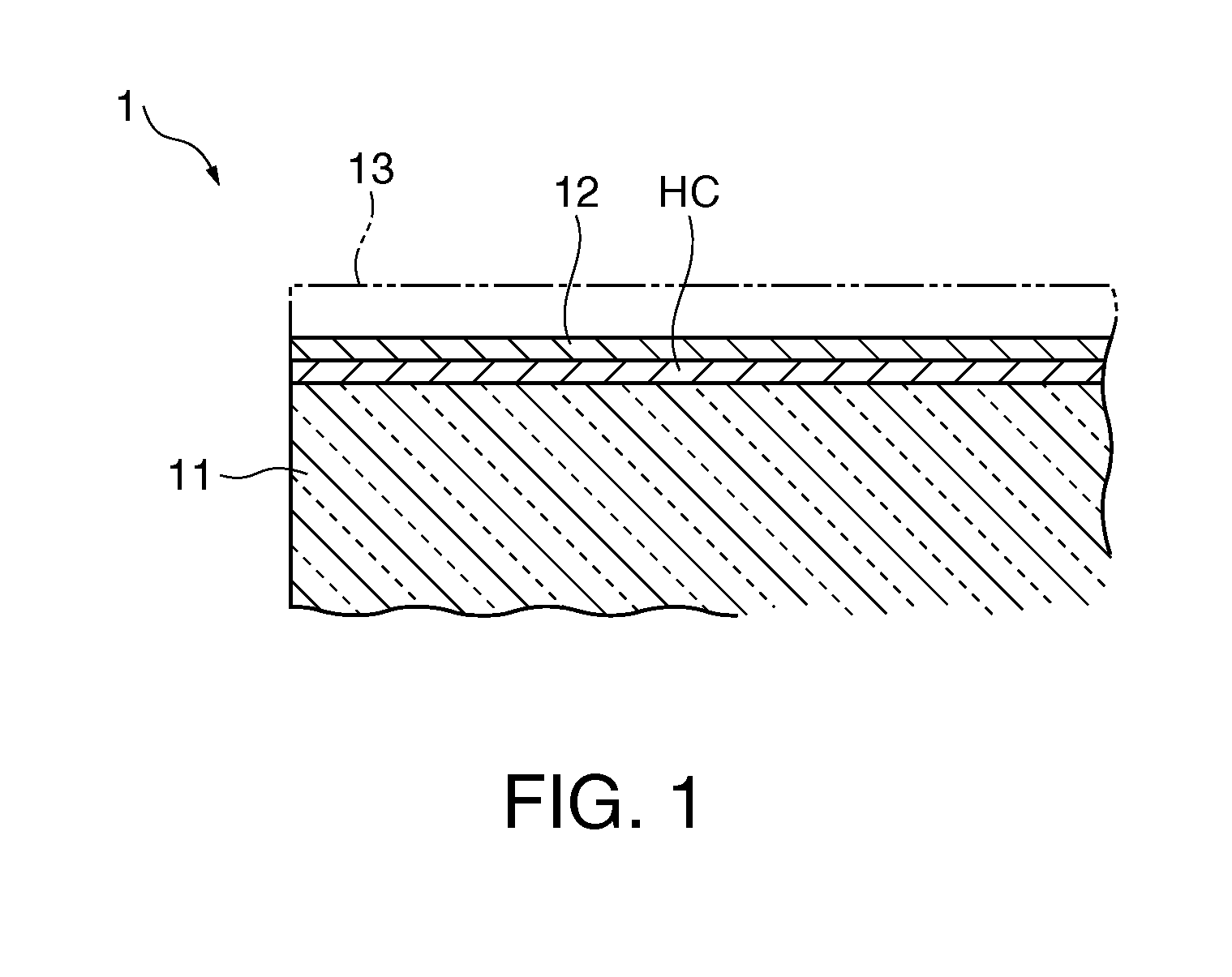
[0042]FIG. 1 is a cross-sectional view of a main part of an optical device 1 according to an embodiment.

[0043]In FIG. 1, the optical device 1 includes a light-transmissive base material 11, a hard coat layer HC provided on a principal surface of the light-transmissive base material 11, and an organic antireflection layer 12 provided on a principal surface of the hard coat layer HC. The organic antireflection layer 12 is provided on either one or both of the two principal surfaces of the light-transmissive base material 11.

[0044]In this embodiment, a water-repellent film 13 may be provided on the organic antireflection layer 12.

[0045]The optical device 1 is a birefringent plate, a lid, or a cover glass to be used in an image-capturing apparatus of a digital camera, or a wave plate or a dust-proof glass to be used in a liquid crystal projector and a pickup apparatus, or other optical devic...


PUM

PropertyMeasurementUnit
thicknessaaaaaaaaaa
refractive indexaaaaaaaaaa

Abstract

An optical device includes an inorganic light-transmissive base material, a hard coat layer, which is provided on a principal surface of the light-transmissive base material and is harder than the light-transmissive base material, and an organic antireflection layer, which is provided on a principal surface of the hard coat layer and contains an organosilicon compound, an epoxy group-containing organic compound, and hollow silica. The hard coat layer and at least one of the organosilicon compound and the epoxy group-containing organic compound are covalently bonded to each other. The occurrence of a defect in the organic antireflection layer can be prevented. The organic antireflection layer has a higher dust-proof effect than an inorganic antireflection film, and therefore, dirt, dust, etc. hardly adhere thereto.

Description

BACKGROUND[0001]1. Technical Field[0002]The present invention relates to an optical device, an image-capturing apparatus including an optical device, an electronic apparatus including an optical device, and a method for producing an optical device.[0003]2. Related Art[0004]An image-capturing apparatus is used in a digital camera, etc. Such an image-capturing apparatus has a structure in which an image-capturing device such as CCD is provided on the bottom of a container, a lid disposed facing the image-capturing device is attached to the container, and an optical low-pass filter along with the lid is disposed facing the image-capturing device.[0005]Some optical devices such as a lid and an optical low-pass filter are configured such that an antireflection film is formed on a light-transmissive substrate composed of an inorganic material.[0006]As the antireflection film, there is known an antireflection film as a related art example which is composed of an inorganic material and is c...

Claims


Application Information

Patent Timeline
Patent Type & Authority Applications(United States)
IPC IPC(8): G02B1/11G02B1/10G02B1/111G02B1/14G02B1/18H01L27/14H01L27/146
CPCG02B1/11G02B1/111G02B1/105G02B1/18G02B1/14
Inventor FURUSATO, DAIKIHOSHINO, YUTA
Owner SEIKO EPSON CORP
Why Eureka
Try Eureka