Optical device, image-capturing apparatus, electronic apparatus, and method for producing optical device

Inactive Publication Date: 2013-10-10
SEIKO EPSON CORP
View PDF6 Cites 0 Cited by
  • Summary
  • Abstract
  • Description
  • Claims
  • Application Information

AI Technical Summary

Benefits of technology

[0031]According to this application example having such a configuration, the organic antireflection layer is formed on the light-transmissive base material by a spin-coating method in which the solution is applied dropwise to the light-transmissive base material and rotating

Problems solved by technology

In the related art disclosed in PTL 1, such a series of complicated and troublesome steps are required, and therefore there is a problem that operational control items are increased, it takes a lot of time and labor to form a film, and as a result, the production cost is increased.
Moreover, there is also a problem that due to particles, dirt, dust, etc. generated during the operations from setting a base material on a jig to vacuuming in a vapor deposition apparatus, a disadvantage that an antireflection film with a defect is formed is caused.
Further, there is also a problem that in the case of using a mixed oxide film obtained by mixing titanium and lanthanum as a material of the antireflection film or the like, uranium (U) or

Method used


Image

  • Optical device, image-capturing apparatus, electronic apparatus, and method for producing optical device
  • Optical device, image-capturing apparatus, electronic apparatus, and method for producing optical device
  • Optical device, image-capturing apparatus, electronic apparatus, and method for producing optical device

Examples


Embodiment Construction

[0041]Embodiments of the invention will be described with reference to the accompanying drawings.

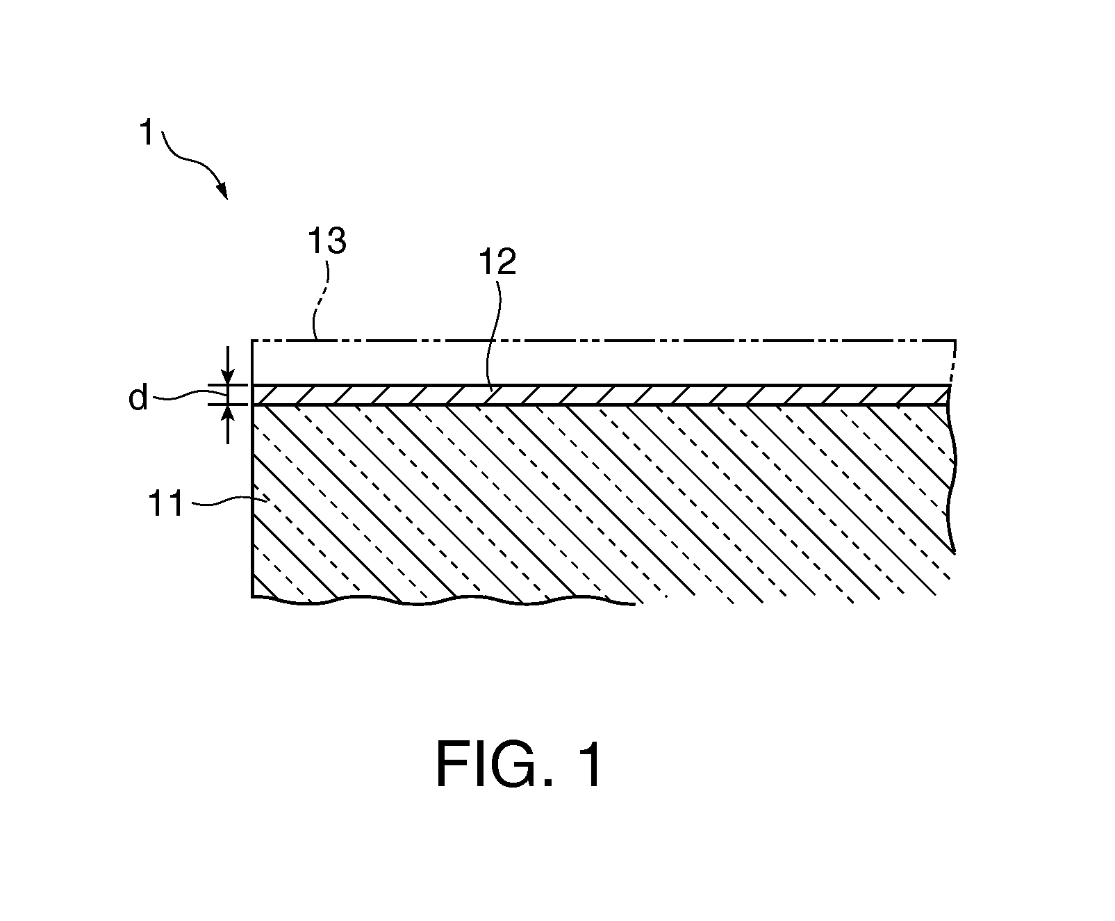
[0042]FIG. 1 is a cross-sectional view of a main part of an optical device 1 according to an embodiment.

[0043]In FIG. 1, the optical device 1 includes a light-transmissive base material 11 and an organic antireflection layer 12 provided directly on a principal surface of the light-transmissive base material 11. The organic antireflection layer 12 is provided on either one or both of the two principal surfaces of the light-transmissive base material 11.

[0044]In this embodiment, a water-repellent film 13 may be provided on the organic antireflection layer 12.

[0045]The optical device 1 is a birefringent plate, a lid, or a cover glass to be used in an image-capturing apparatus of a digital camera, or a wave plate or a dust-proof glass to be used in a liquid crystal projector and a pickup apparatus, or other optical device.

1. Light-Transmissive Base Material

[0046]The light-transmissive base m...


PUM

PropertyMeasurementUnit
Thicknessaaaaaaaaaa
Thicknessaaaaaaaaaa
Lightaaaaaaaaaa

Abstract

An optical device is configured such that the device includes an inorganic light-transmissive base material and an organic antireflection layer, which is provided on a principal surface of the light-transmissive base material and contains an organosilicon compound, an epoxy group-containing organic compound, and hollow silica, and the light-transmissive base material and at least one of the organosilicon compound and the epoxy group-containing organic compound are covalently bonded to each other. Since dirt, dust, etc. do not adhere to a principal surface of the light-transmissive base material during film formation, the occurrence of a defect in the organic antireflection layer can be prevented. The organic antireflection layer has a larger contact angle than an antireflection layer made of an inorganic material, and therefore has a higher dust-proof effect than an inorganic antireflection layer, and thus, dirt, dust, etc. hardly adhere thereto.

Description

BACKGROUND[0001]1. Technical Field[0002]The present invention relates to an optical device, an image-capturing apparatus including an optical device, an electronic apparatus including an optical device, and a method for producing an optical device.[0003]2. Related Art[0004]An image-capturing apparatus is used in a digital camera, etc. Such an image-capturing apparatus has a structure in which an image-capturing device such as CCD is provided on the bottom of a container, a lid disposed facing the image-capturing device is attached to the container, and an optical low-pass filter along with the lid is disposed facing the image-capturing device.[0005]Some optical devices such as a lid and an optical low-pass filter are configured such that an antireflection film is formed on a light-transmissive substrate composed of an inorganic material.[0006]As the antireflection film, there is known an antireflection film as a related art example which is composed of an inorganic material and is c...

Claims


Application Information

Patent Timeline
IPC IPC(8): G02B1/11G02B1/111G02B1/18H01L27/14H01L27/146
CPCG02B1/11G02B1/04G02B1/111G02B2207/107C08L83/04C08L63/00C08L27/12
Inventor FURUSATO, DAIKIHOSHINO, YUTA
Owner SEIKO EPSON CORP
Why Eureka
Try Eureka