Resistance change memory device having threshold switching and memory switching characteristics, method of fabricating the same, and resistance change memory device including the same

a resistance change memory and threshold switching technology, applied in the field of resistive change memory devices, can solve the problems of diodes not suitable and the transistor has a limit in size reduction, and achieve the effect of increasing process steps and high degree of integration

Active Publication Date: 2013-10-17
GWANGJU INST OF SCI & TECH
View PDF7 Cites 10 Cited by
  • Summary
  • Abstract
  • Description
  • Claims
  • Application Information

AI Technical Summary

Benefits of technology

[0008]An aspect of the present invention is to provide a resistance change memory device and a resistance change memory array, which include selection device characteristics and can be fabricated in a high degree of integration without substantially increasing process steps.

Problems solved by technology

However, the transistor has a limit in size reduction due to a short channel effect such as punch through.
In addition, since the diode allows only unidirectional electric current, the diode is not suitable for a bipolar device which exhibits resistance change characteristics at both polarities as in the resistance change device.

Method used


Image

  • Resistance change memory device having threshold switching and memory switching characteristics, method of fabricating the same, and resistance change memory device including the same
  • Resistance change memory device having threshold switching and memory switching characteristics, method of fabricating the same, and resistance change memory device including the same
  • Resistance change memory device having threshold switching and memory switching characteristics, method of fabricating the same, and resistance change memory device including the same

Examples


example 1

Preparative Example 1

Preparation of Memory Switching Device

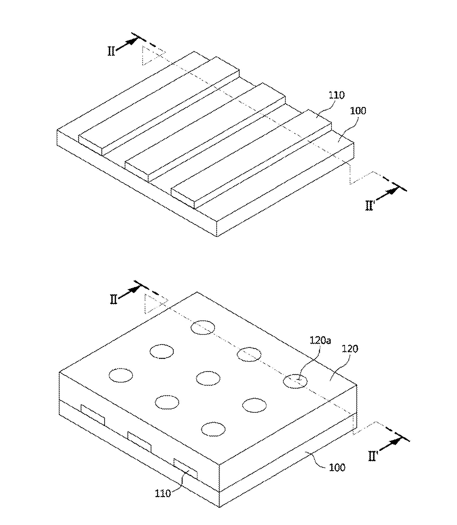
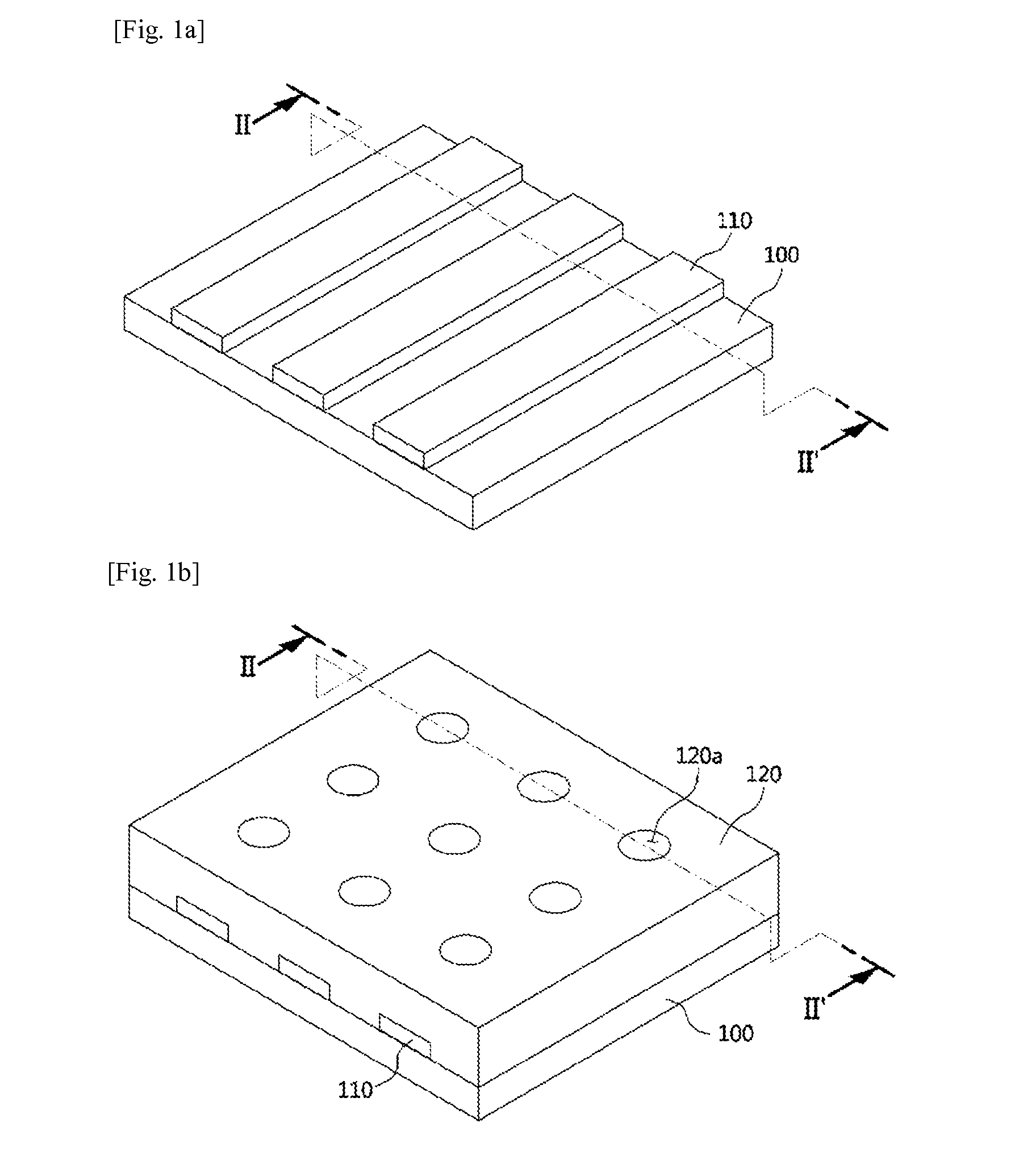
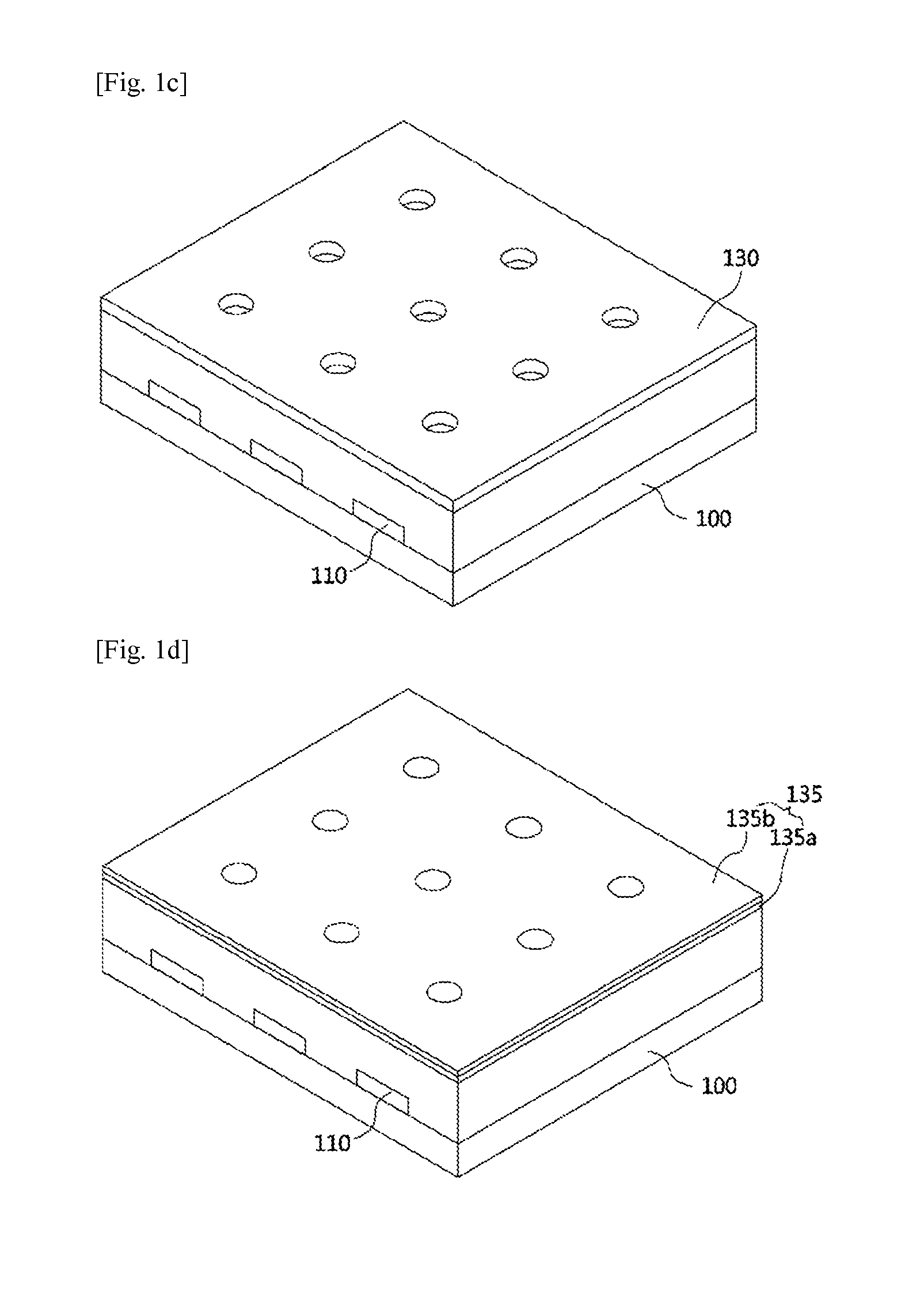
[0070]A 50 nm thick Pt layer was formed on a substrate to provide a first electrode by RF magnetron sputtering. Next, a silicon oxide layer was formed to a thickness of about 100 nm, and holes having a diameter of about 250 nm were formed in the silicon oxide layer to expose the Pt layer therethrough. On the Pt layer exposed through the holes and the silicon oxide layer, an Nb layer was deposited to a thickness of about 10 nm by sputtering, and subjected to oxygen treatment at an oxygen partial pressure of 50 sccm and at 500° C. for 10 minutes by RTA to form a metal oxide layer. Next, an about 40 nm thick W layer was formed on the oxygen treated Nb layer to provide a second electrode by sputtering.

example 2

Preparative Example 2

Preparation of Threshold Switching Device

[0071]A 50 nm thick Pt layer was formed on a substrate to provide a first electrode by RF magnetron sputtering. Next, a silicon oxide layer was formed to a thickness of about 100 nm, and holes having a diameter of about 250 nm were formed in the silicon oxide layer to expose the Pt layer therethrough. An NbO2-x layer was deposited to a thickness of 10 nm on the Pt layer exposed through the holes and the silicon oxide layer by reactive sputtering at 2 sccm and at 500° C. for 10 minutes. Next, an about 40 nm thick W layer was formed on the NbO2-x layer to provide a second electrode by sputtering.

example 3

Preparative Example 3

Preparation of Hybrid Device

[0072]A 50 nm thick Pt layer was formed on a substrate to provide a first electrode by RF magnetron sputtering. Next, a silicon oxide layer was formed to a thickness of about 100 nm, and holes having a diameter of about 250 nm were formed in the silicon oxide layer to expose the Pt layer therethrough. An NbO2-x layer was deposited to a thickness of 10 nm on the Pt layer exposed through the holes and the silicon oxide layer by reactive sputtering at 2 sccm and at 500° C. for 10 minutes. Then, the NbO2-x is exposed to air for oxygen treatment. Next, an about 40 nm thick W layer was formed on the NbO2-x layer to provide a second electrode by sputtering.

[0073]FIG. 7a is a graph depicting an analysis result of compositions of the respective layers of the memory switching device of Preparative Example 1, and FIG. 7b is a current-voltage curve of the memory switching device of Preparative Example 1.

[0074]Referring to FIG. 7a, the metal oxide...


PUM


Abstract

Disclosed are a resistance change memory device, a method of fabricating the same, and a resistance change memory array including the same. The resistance change memory device includes a first electrode and a second electrode. A hybrid switching layer is interposed between the first electrode and the second electrode. The hybrid switching layer is a metal oxide layer having both threshold switching characteristics and memory switching characteristics.

Description

CROSS-REFERENCE TO RELATED APPLICATION[0001]This application claims priority to Korean Patent Application No. 10-2012-0039566 filed on 17 Apr. 2012 and all the benefits accruing therefrom under 35 U.S.C. §119, the contents of which are incorporated by reference in their entirety.BACKGROUND[0002]1. Technical Field[0003]The present invention relates to semiconductor devices, and more particularly, to resistance change memory devices.[0004]2. Description of the Related Art[0005]Currently, a flash memory device commercialized as a resistance change memory device is based on change in threshold voltage resulting from storage or removal of charges from a charge storage layer. The charge storage layer may be a floating gate formed of a polysilicon layer or a charge trap layer formed of a silicon nitride layer. Recently, studies have been made to develop next generation resistance change memory devices which have lower power consumption and a higher degree of integration than the flash memo...

Claims


Application Information

Patent Timeline
Patent Type & Authority Applications(United States)
IPC IPC(8): H01L45/00
CPCH01L45/145H01L45/1608H10B63/82H10B63/80H10N70/24H10N70/041H10N70/026H10N70/826H10N70/8833H10N70/20H10N70/883H10N70/021
Inventor HWANG, HYUNSANGKIM, SEONGHYUNLIU, XINJUN
Owner GWANGJU INST OF SCI & TECH
Why Eureka
Try Eureka