Nanofiber manufacturing device

a manufacturing device and nanofiber technology, applied in the field of nanofiber manufacturing equipment, can solve the problems of difficult continuous operation of the electrospinning device, increased leak current to an undesirable level, and caused by the breakdown of the insulation between the collector and the case and other members, and achieve the effect of stably producing nanofibers, simple structure and shap

Inactive Publication Date: 2013-10-17
TOPTEC +1
View PDF9 Cites 19 Cited by
  • Summary
  • Abstract
  • Description
  • Claims
  • Application Information

AI Technical Summary

Benefits of technology

[0033]According to the present invention, there is provided the nanofiber manufacturing apparatus wherein since the case or the nozzle block is grounded, all of the nozzle block, the material tank in which the polymer solution is stored before the ejection from the nozzles, and polymer solution transferring instruments (for example, pipes or pumps) for transferring the polymer solution to the nozzle block from the material tank become ground potentials, thereby removing the need to provide high potential voltage specifications to the material tank or the polymer solution transferring instruments, in the same manner as the electrospinning device as disclosed in the cited document. Accordingly, the complication of the electrospinning unit, which is caused by the high potential voltage specifications of the material tank or the polymer solution transferring instruments, can be prevented.
[0034]According to the present invention, when the collector is seen from the nozzle block, if it is assumed that the thickness of the insulation member is a and the distance between the outer edge of the insulation member and the outer edge of the collector is b, it is satisfied that a≧6 mm and a+b≧50 mm, so that the insulation state between the collector and the case or other members is sufficiently good, and as will be apparent from the examples as will be explained later, even if a voltage of 35 kV is applied between the nozzle block and the collector to conduct the electrospinning, the insulation breakdown between the collector and the case or other members does not occur. Further, leak current is limited to a given range. As a result, possibilities where the operations of the electrospinning units stop are reduced to an extremely low level, so that the electrospinning units can be continuously operated for long hours to stably produce the nanofibers having desired performance in large quantities.
[0035]According to the present invention, further, the leak current is limited to the given range, so that the current supplied form the power supply is always monitored, thereby allowing the trouble of each electrospinning unit to be early found.
[0036]According to the present invention, further, the power supply is configured to have one side electrode connected to the collector and the other side electrode connected to the nozzle block and at the same time having ground potential, so that in the same manner as the electrospinning device as disclosed in the cited document, while a high voltage is being applied to the collector made in a relatively simple structure and shape in the state where the nozzle block having a relatively complicate structure and shape is grounded, the electrospinning is conducted in stable conditions, without having any discharging or voltage drop. According to the present invention, further, the auxiliary belt unit includes the auxiliary belt formed of the insulative porous endless belt located and freely rotated at a position encompassing the collector and the auxiliary belt driver adapted to rotate the auxiliary belt to a rotating speed corresponding to the conveying speed of the long sheet, so that even if large electrostatic attraction between the collector and the long sheet occurs, the auxiliary belt exists between the long sheet and the collector to prevent the long sheet from being pulled toward the collector or to avoid the interference in the gentle conveying of the long sheet. Accordingly, it is possible to conduct the electrospinning of the nanofibers under the uniform conditions, and of course, the operation itself of the electrospinning units does not stop at all. Further, it is possible to produce the nanofibers having uniform qualities (for example, in the diameters of nanofibers, in the distribution of the diameters of nanofibers, in the accumulation quantities of nanofibers, in the thickness of nanofiber non-woven fabric, and in the air permeability of nanofiber non-woven fabric and so on) in large quantities.
[0037]According to the present invention, further, the auxiliary belt is rotated to the rotating speed corresponding to the conveying speed of the long sheet, so that the existence of the auxiliary belt gives no bad influence on the conveying state of the long sheet. Also, the auxiliary belt of each electrospinning unit is formed of the insulative porous endless belt, thereby giving no big influences on the distribution of the electric field between the collector and the nozzle block.
[0038]According to the present invention, further, the auxiliary belt can be reliably rotated at the rotating speed corresponding to the conveying speed of the long sheet. Also, the inclination of one auxiliary belt roller is appropriately controlled and the position of the auxiliary belt with respect to the width direction of the auxiliary belt roller is precisely controlled for long hours.

Problems solved by technology

According to the electrospinning device 900 disclosed in the cited document, however, the insulation between the collector and the case and other members is not sufficiently formed, and so as to manufacture the nanofibers having desired performance, thus, if the electrospinning is conducted through the application of an extremely high voltage (for example, 35 kV) between the nozzle block and the collector, the insulation breakdown between the collector and the case and other members is caused.
Even if the insulation breakdown does not occur, leak current may be increased to an undesirable level.
As a result, the operation of the electrospinning device should stop, which makes it hard to continuously operate the electrospinning device for long hours, and furthermore, it is difficult to stably produce the nanofibers having the desired performance in large quantities.
According to the electrospinning device 900 disclosed in the cited document, additionally, since the high voltage is applied to the collector, large electrostatic attraction between the collector and the collection base material occurs to cause the base material to be pulled toward the collector, which fails to the gentle conveying of the base material.
Accordingly, it is hard to conduct the electrospinning of the nanofibers under the uniform conditions for long hours, and of course, the operation itself of the electrospinning device should stop.
Further, it is impossible to produce the nanofibers having uniform qualities (for example, in the mean diameters of nanofibers, in the distribution of the diameters of nanofibers, in the accumulation quantities of nanofibers, in the thicknesses of nanofiber layers, and in the air permeability of nanofiber layers and so on) in large quantities.

Method used


Image

  • Nanofiber manufacturing device
  • Nanofiber manufacturing device
  • Nanofiber manufacturing device

Examples


first embodiment

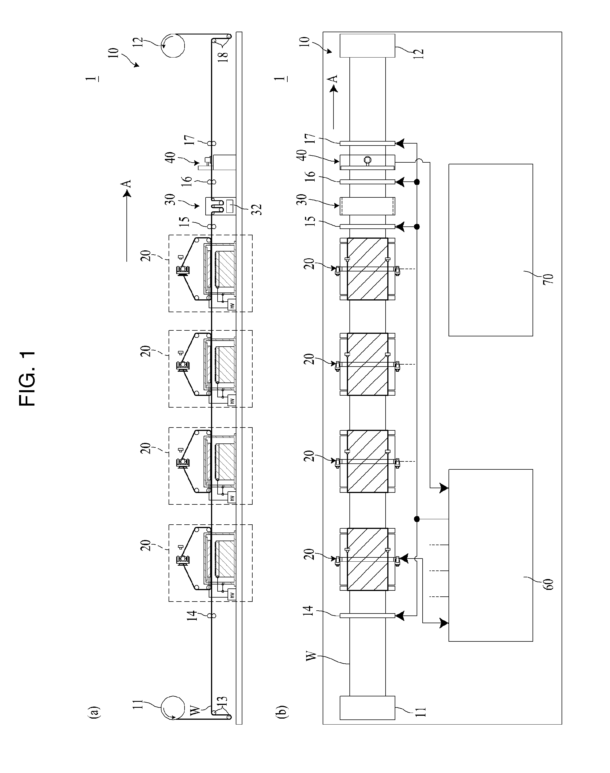
[0098]FIGS. 1a and 1b are front and plan views showing a nanofiber manufacturing apparatus according to a first embodiment of the present invention. FIG. 1a is a front view showing the nanofiber manufacturing apparatus 1 and FIG. 1b is a plan view showing the nanofiber manufacturing apparatus 1. In FIGS. 1a and 1b, a polymer solution supply unit and a polymer solution collection unit are not shown. Further, some parts of FIG. 1a are shown in FIG. 2.

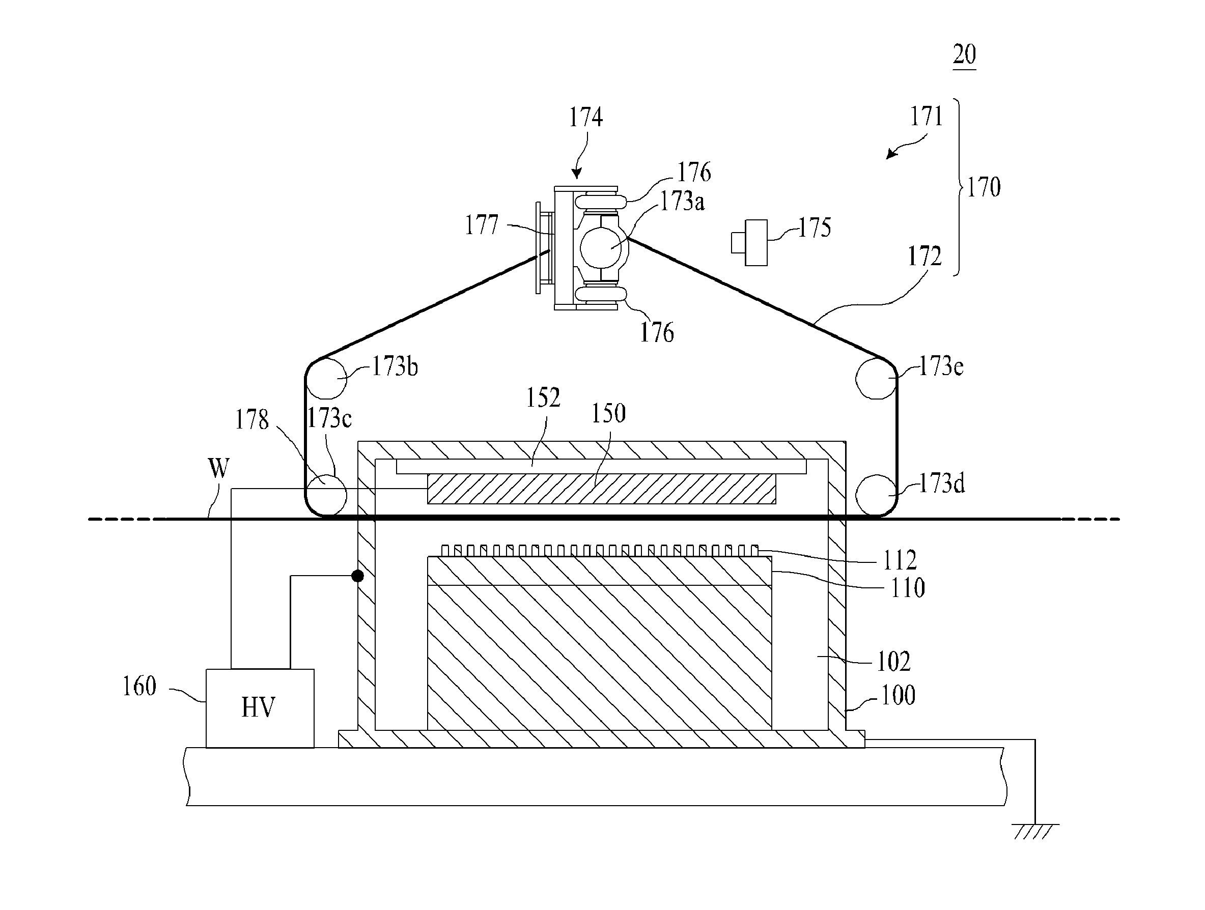
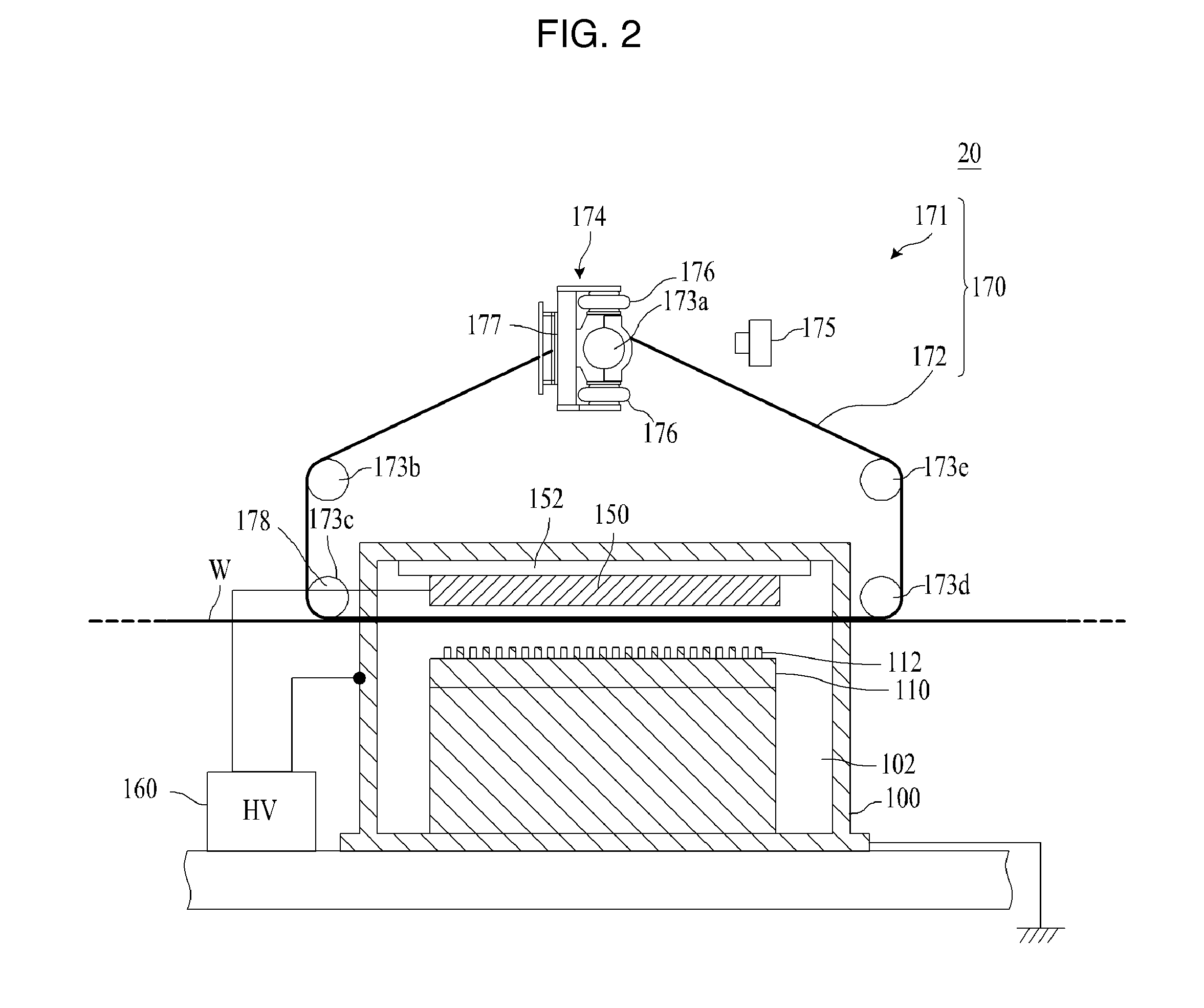
[0099]FIG. 2 is a sectional view showing an electrospinning unit used in the nanofiber manufacturing apparatus according to the first embodiment of the present invention.

[0100]FIGS. 3a and 3b are enlarged sectional and plan views showing the main parts of the electrospinning unit, wherein FIG. 3a is an enlarged sectional view showing the main parts of the electrospinning unit and FIG. 3b is an enlarged plan view showing the main parts of the electrospinning unit. FIG. 4 is a sectional view showing an auxiliary belt unit moved in a conveyi...

example 1

[0134]Example 1 is the experimental example clearly showing the appropriate thickness a of the insulation member 152, so as to stop the leak current at the given range. Table 1 shows the experimental results of the example 1, and FIG. 8 is a graph showing the experimental results of the example 1.

TABLE 1a =a =a = 5 mma = 6 mma = 8 mm10 mm12 mmmAkVmAkVmAkVmAkVmAkV0.0129.80.0137.20.0141.00.0143.00.0146.30.0234.40.0244.30.0246.60.0249.00.0254.00.030.0349.10.0354.80.0356.00.0359.00.040.0450.30.0459.70.040.04Insu-36.053.4lationBreak-down*b is fixed to 30 mm

[0135]In the example 1, in the state where the polymer solution was not fed to the nozzle block 110 in the nanofiber manufacturing apparatus 1 according to the present invention (wherein, the thickness a was set to 5 mm, 6 mm, 8 mm, 10 mm or 12 mm, and the distance b was fixed to 30 mm), the voltage was applied between the collector 150 and the nozzle block 110 to allow a given current supplied from the power supply 160 to become a giv...

example 2

[0137]Example 2 is the experimental example clearly showing the appropriate distance a+b between the insulation member 152 and the collector 150, so as to stop the leak current at the given range. Table 2 shows the experimental results of the example 2, and FIG. 9 is a graph showing the experimental results of the example 2.

TABLE 2mAkVmAkVmAkVmAkVa + b =a + b =a + b =a + b =45 mm50 mm60 mm80 mm0.0132.20.0137.00.0139.20.0140.30.0234.80.0237.30.0250.20.0250.70.0336.30.0340.80.030.0353.00.0437.00.0442.60.040.0456.50.05—0.05—0.050.05Insulation—46.054.058.8Break-downa + b =a + b =a + b =a + b =100 mm120 mm140 mm160 mm0.0141.20.0141.70.0141.80.0142.80.0250.90.0252.70.0255.30.0257.10.0354.80.0360.30.0360.50.0360.80.0457.30.04—0.04—0.04—0.0560.70.05—0.05—0.05—Insulation————Break-down*a is fixed to 40 mm

[0138]In the example 2, in the state where the polymer solution was not fed to the nozzle block 110 in the nanofiber manufacturing apparatus 1 according to the present invention (wherein, the...


PUM

PropertyMeasurementUnit
angleaaaaaaaaaa
angleaaaaaaaaaa
voltageaaaaaaaaaa

Abstract

The present invention relates to a nanofiber manufacturing apparatus having a plurality of electrospinning units disposed serially along the conveying direction of a long sheet, each electrospinning unit including: a conductive case; a collector attached to the case by means of an insulation member; a nozzle block disposed to face the collector and having a plurality of nozzles from which polymer solution is ejected mounted thereon; a power supply adapted to apply a high voltage to a space between the collector and the nozzle block; an auxiliary belt formed of an insulative porous endless belt located and freely rotated at a position encompassing the collector; and an auxiliary belt driver adapted to rotate the auxiliary belt to a rotating speed corresponding to the conveying speed of the long sheet, wherein the positive electrode of the power supply is connected to the collector, and the negative electrode thereof to the nozzle block and the case, and when the collector is seen from the nozzle block, the outer edge of the insulation member is located more outwardly than the outer edge of the collector, so that if it is assumed that the thickness of the insulation member is a and the distance between the outer edge of the insulation member and the outer edge of the collector is b, it is satisfied that a≧6 mm and a+b≧50 mm.

Description

CROSS REFERENCE RELATED APPLICATION[0001]This application claims foreign priority of Japanese Patent Application No. 2010-272078, filed on Dec. 6, 2010 and Korean Patent Application No. 10-2011-0017376, filed on Feb. 25, 2011, which are incorporated by reference in their entirety into this application.TECHNICAL FIELD[0002]The present invention relates to a nanofiber manufacturing apparatus.BACKGROUND ART[0003]In conventional practices, there is proposed a nanofiber manufacturing apparatus having a plurality of electrospinning units located along a given conveying direction in which a long sheet is conveyed. Further, as the electrospinning devices used in such nanofiber manufacturing apparatus, there has been proposed Japanese Patent No. 2008-506864 (hereinafter, referred to as cited document) wherein each electrospinning device applies a high voltage to a collector in the state where a nozzle block is grounded, thereby conducting electrospinning.[0004]FIG. 30 shows an electrospinnin...

Claims


Application Information

Patent Timeline
Patent Type & Authority Applications(United States)
IPC IPC(8): D01D5/00
CPCD01D5/0076B82Y30/00B82Y40/00D01D1/06D01D5/0061D01D5/0069D01D13/00D01D13/02D01F13/00Y02P70/62D01D4/00D01D5/00
Inventor LEE, JAE HWAN
Owner TOPTEC
Why Eureka
Try Eureka