

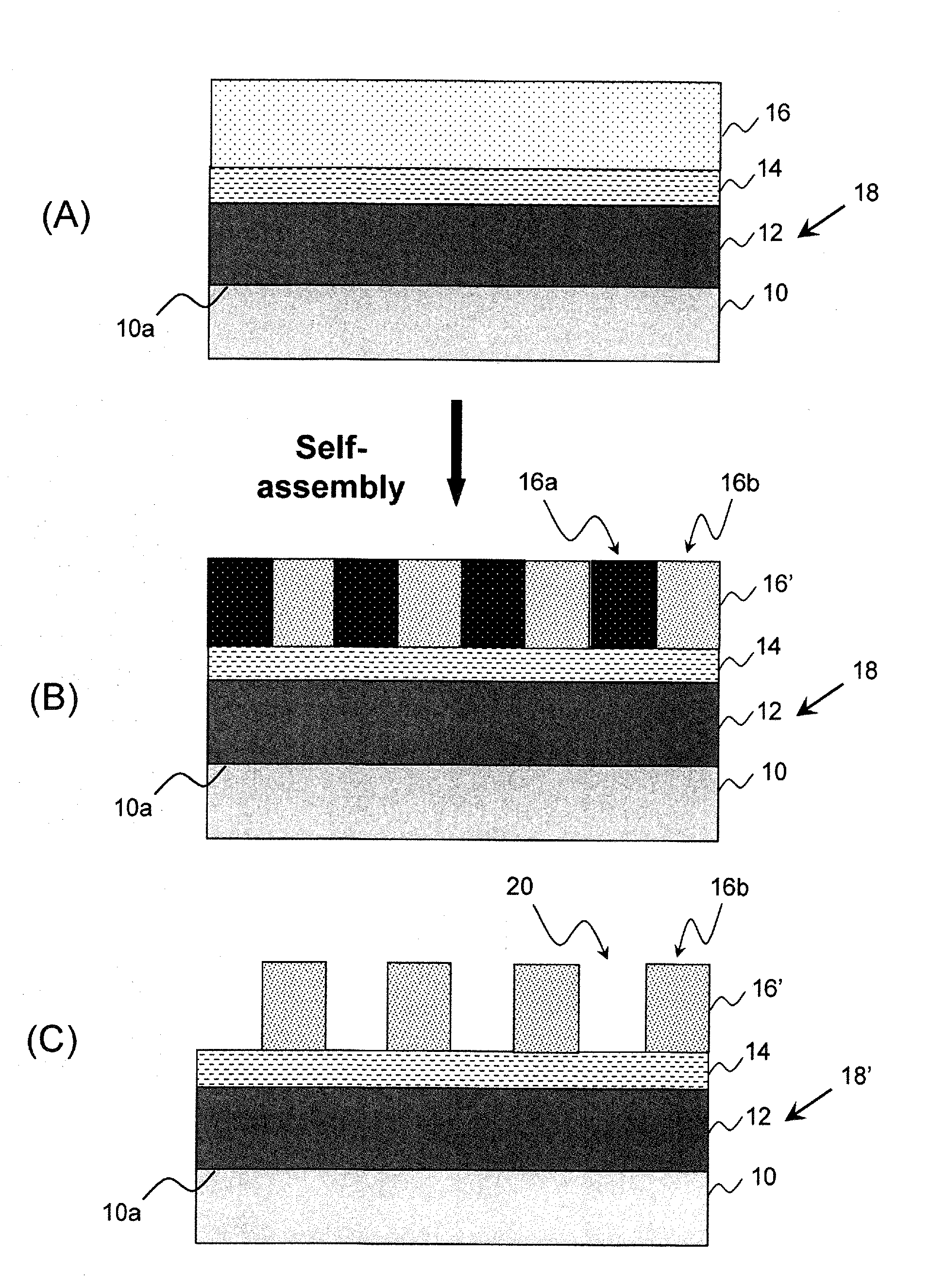
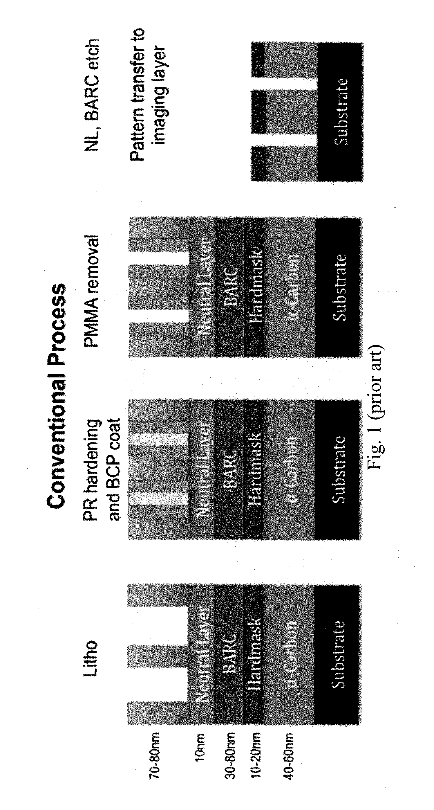
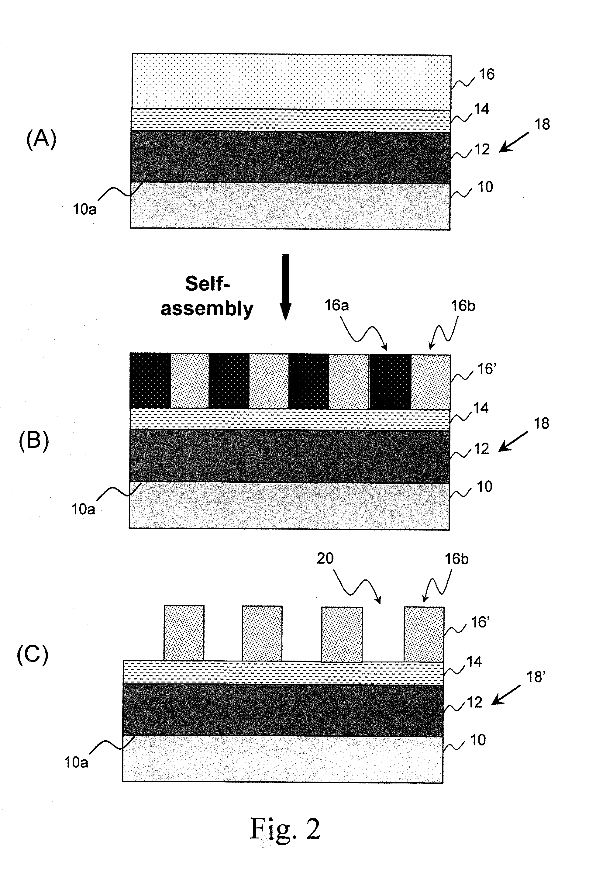
Silicon hardmask layer for directed self-assembly
- Summary
- Abstract
- Description
- Claims
- Application Information
AI Technical Summary
Benefits of technology
Problems solved by technology
Method used
Image

Examples
example 1
Synthesis of Polymer 1
[0060]In this Example, a silicon hardmask copolymer was synthesized by adding 8.01 grams of phenethyltrimethoxysilane (Gelest Inc, Morrisville, Pa.), 5.33 grams of 2-(carbomethoxy)ethyltrimethoxysilane (Gelest Inc.), and 60.11 grams of PGMEA (Ultra Pure Solutions, Inc., Castroville, Calif.) to a two-neck round-bottom flask. Over a 5-minute period, 5.50 grams of a 3N acetic acid solution (17.6% acetic acid in water, Aldrich, St Louis, Mo.) was added to the flask while the solution was being stirred. The round-bottom flask was fitted with a distillation head, distillation column, and collection flask. The solution was heated at 97.5° C. for 6.5 hours to complete the reaction and then allowed to cool down to room temperature. A total 64.8 grams of solution was collected and estimated solids content was 15.00%.
example 2
Synthesis of Hardmask 1
[0061]A hardmask formulation was prepared by mixing 4.00 grams of Polymer 1 with 1.50 grams of a 0.4% solution in PGME of benzyltriethylammonium chloride (BTEAC, Aldrich), 18.40 grams of PGME, and 16.50 grams of PGMEA to make a 1.50% solids solution. The formulation was spin-coated onto a 4-inch silicon wafer at 1,500 rpm for 60 seconds followed by baking on a hotplate at 230° C. for 60 seconds. This process yielded a ˜400 Å film.
example 3
Synthesis of Polymer 2
[0062]
[0063]In this Example, a silicon copolymer was synthesized by adding 8.00 grams of phenethyltrimethoxysilane, 5.45 grams of 2-(carbomethoxy)ethyltrimethoxysilane, and 3.19 grams of tetraethoxysilane (Gelest Inc.), to 60.70 grams of PGME in a two-neck round-bottom flask. Over a 5-minute period, 6.91 grams of a 3N acetic acid solution (17.6% acetic acid in water) were added to the flask while the solution was being stirred. The round-bottom flask was fitted with a distillation head, distillation column, and collection flask. The solution was heated at 97.5° C. for 6.0 hours to complete the reaction and then allowed to cool down to room temperature. A total 68.0 grams of solution was collected and estimated solids content was 15.78%.
PUM
| Property | Measurement | Unit |
|---|---|---|
| Size | aaaaa | aaaaa |
| Composition | aaaaa | aaaaa |
| Structure | aaaaa | aaaaa |
Abstract
Description
Claims
Application Information