Method for manufacturing a hybrid integrated component

Active Publication Date: 2013-10-24
ROBERT BOSCH GMBH
View PDF6 Cites 29 Cited by
  • Summary
  • Abstract
  • Description
  • Claims
  • Application Information

AI Technical Summary

Benefits of technology

[0006]The present invention provides a simple and cost-effective manufacturing method for hybrid integrated components including at least one MEMS element,

Problems solved by technology

Thus, the use of three starting substrates during the manufacture of the three component elements causes a relatively high material and processing outlay.
In addi

Method used


Image

  • Method for manufacturing a hybrid integrated component
  • Method for manufacturing a hybrid integrated component
  • Method for manufacturing a hybrid integrated component

Examples


Embodiment Construction

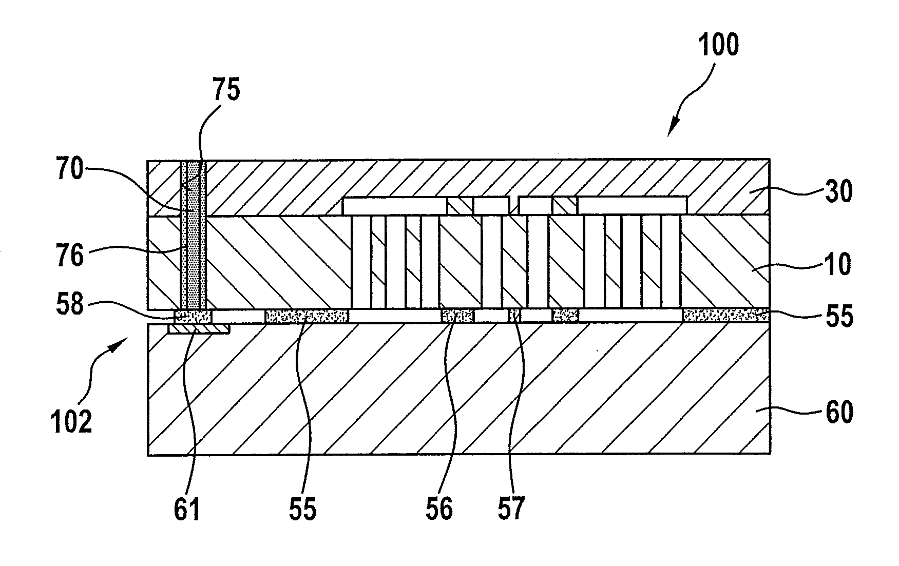
[0024]The method according to the present invention for manufacturing a hybrid integrated component proceeds from two semiconductor substrates, which are processed independently of one another. At least parts of a signal processing and evaluation circuit for the component are advantageously integrated on the one semiconductor substrate, which is referred to hereafter as the ASIC substrate. Furthermore, through contacts, so-called TSVs (through silicon vias), may be applied in the ASIC substrate, for example, in the form of pocket holes filled with tungsten or copper. These TSVs are used for the external electrical contacting of the component within the scope of the second-level assembly. The CMOS processing of the ASIC substrate is not described in detail here, however, since it is not specified in greater detail by the present invention.

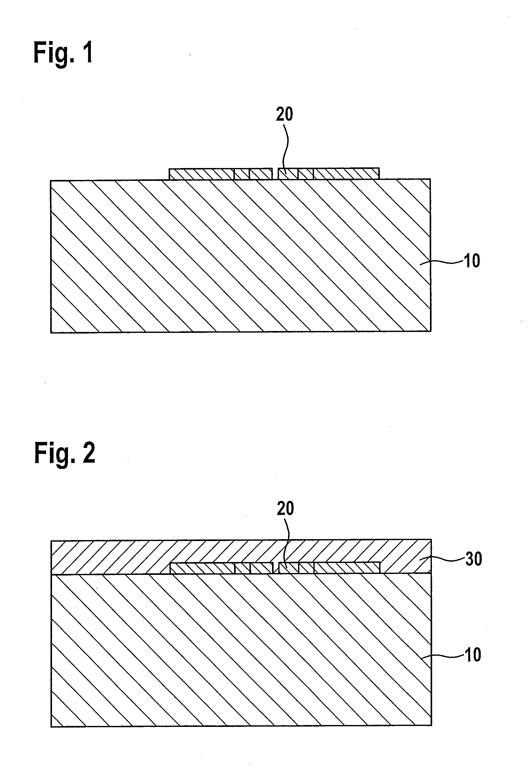
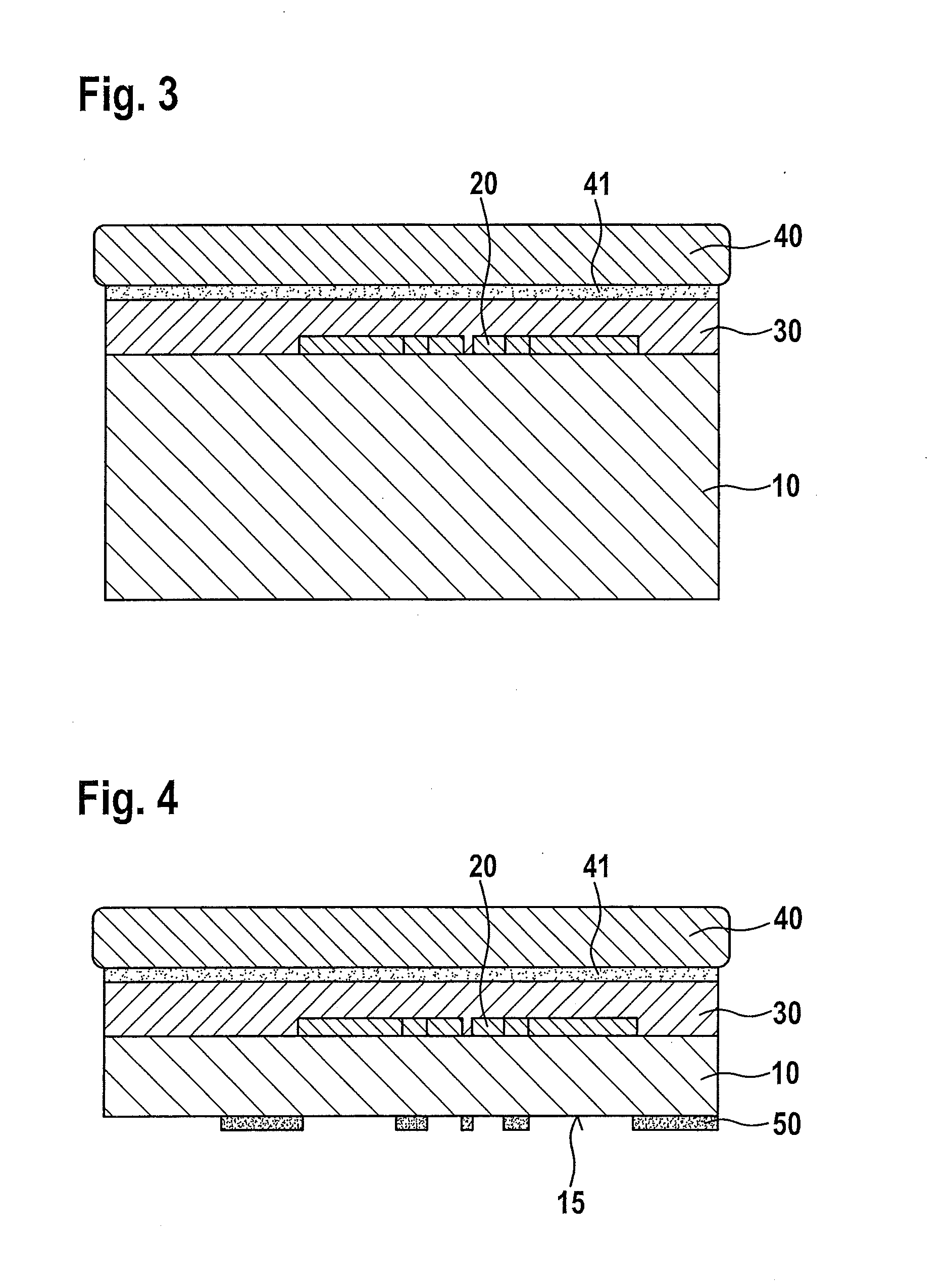
[0025]The other semiconductor substrate 10, which is also referred to hereafter as the MEMS substrate, is shown in FIG. 1. In the exemplary embodim...


PUM

PropertyMeasurementUnit
Electrical conductivityaaaaaaaaaa
Structureaaaaaaaaaa
Mechanical propertiesaaaaaaaaaa

Abstract

A simple and cost-effective manufacturing method for hybrid integrated components including at least one MEMS element, a cap for the micromechanical structure of the MEMS element, and at least one ASIC substrate, using which a high degree of miniaturization may be achieved. The micromechanical structure of the MEMS element and the cap are manufactured in a layered structure, proceeding from a shared semiconductor substrate, by applying at least one cap layer to a first surface of the semiconductor substrate, and by processing and structuring the semiconductor substrate proceeding from its other second surface, to produce and expose the micromechanical MEMS structure. The semiconductor substrate is then mounted with the MEMS-structured second surface on the ASIC substrate.

Description

RELATED APPLICATION INFORMATION[0001]The present application claims priority to and the benefit of German patent application no. 10 2012 206 732.9, which was filed in Germany on Apr. 24, 2012, the disclosure of which is incorporated herein by reference.FIELD OF THE INVENTION[0002]The present invention relates to a method for manufacturing a hybrid integrated component including at least one MEMS (micro-electromechanical systems) element, a cap for the micromechanical structure of the MEMS element, and at least one ASIC (application specific integrated circuit) substrate.BACKGROUND INFORMATION[0003]A method for manufacturing a vertically integrated component having an MEMS element, a cap for the micromechanical structure of the MEMS element, and an ASIC substrate is discussed in US 2011 / 0012247 A1. The method provides that these three elements of the component are manufactured independently of one another and a separate starting substrate is provided for each element. The MEMS substr...

Claims


Application Information

Patent Timeline
IPC IPC(8): B81C1/00B81B7/00
CPCB81C1/00269B81B7/007B81C1/00238B81C2203/0785
Inventor FREY, JENSFISCHER, FRANK
Owner ROBERT BOSCH GMBH
Why Eureka
Try Eureka