

Semiconductor device and method of manufacturing same
a semiconductor chip and semiconductor technology, applied in the field of semiconductor chips, can solve the problems of low power cycle resistance easy reduction of the joint temperature of the chip to the upper limit, and hardly expected heat dissipation from the upper surface of the semiconductor chip, so as to improve the visibility of the camera and reduce the false detection of sections
- Summary
- Abstract
- Description
- Claims
- Application Information
AI Technical Summary
Benefits of technology
Problems solved by technology
Method used
Image

Examples
first embodiment
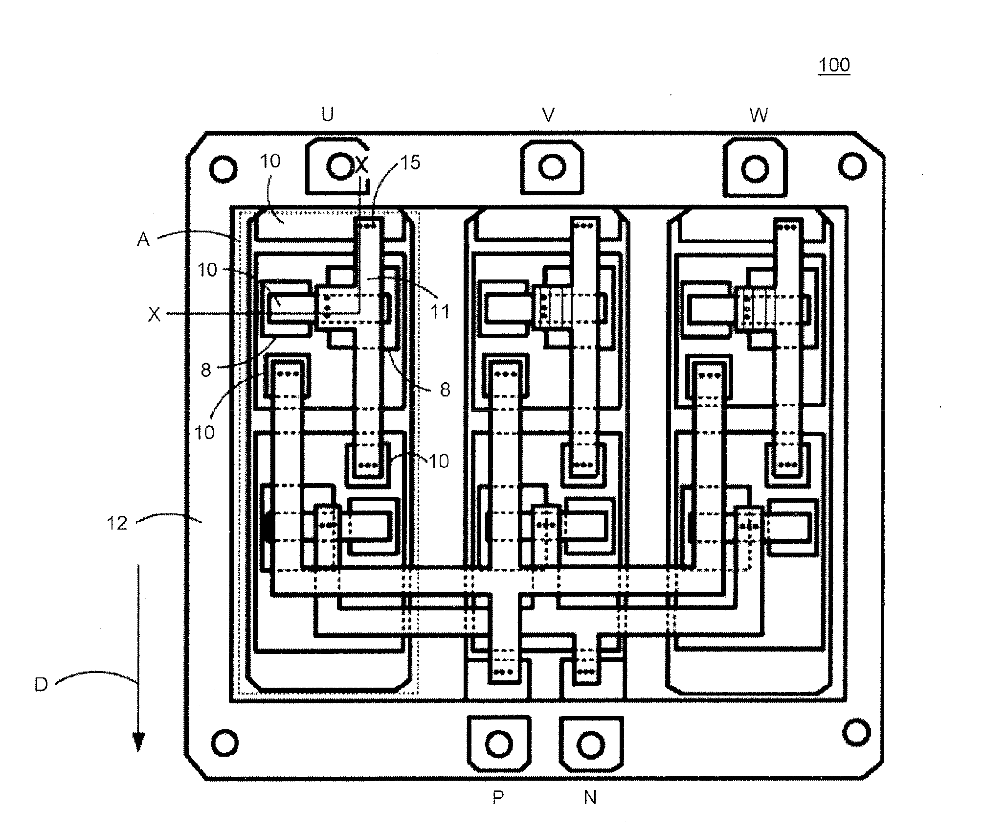
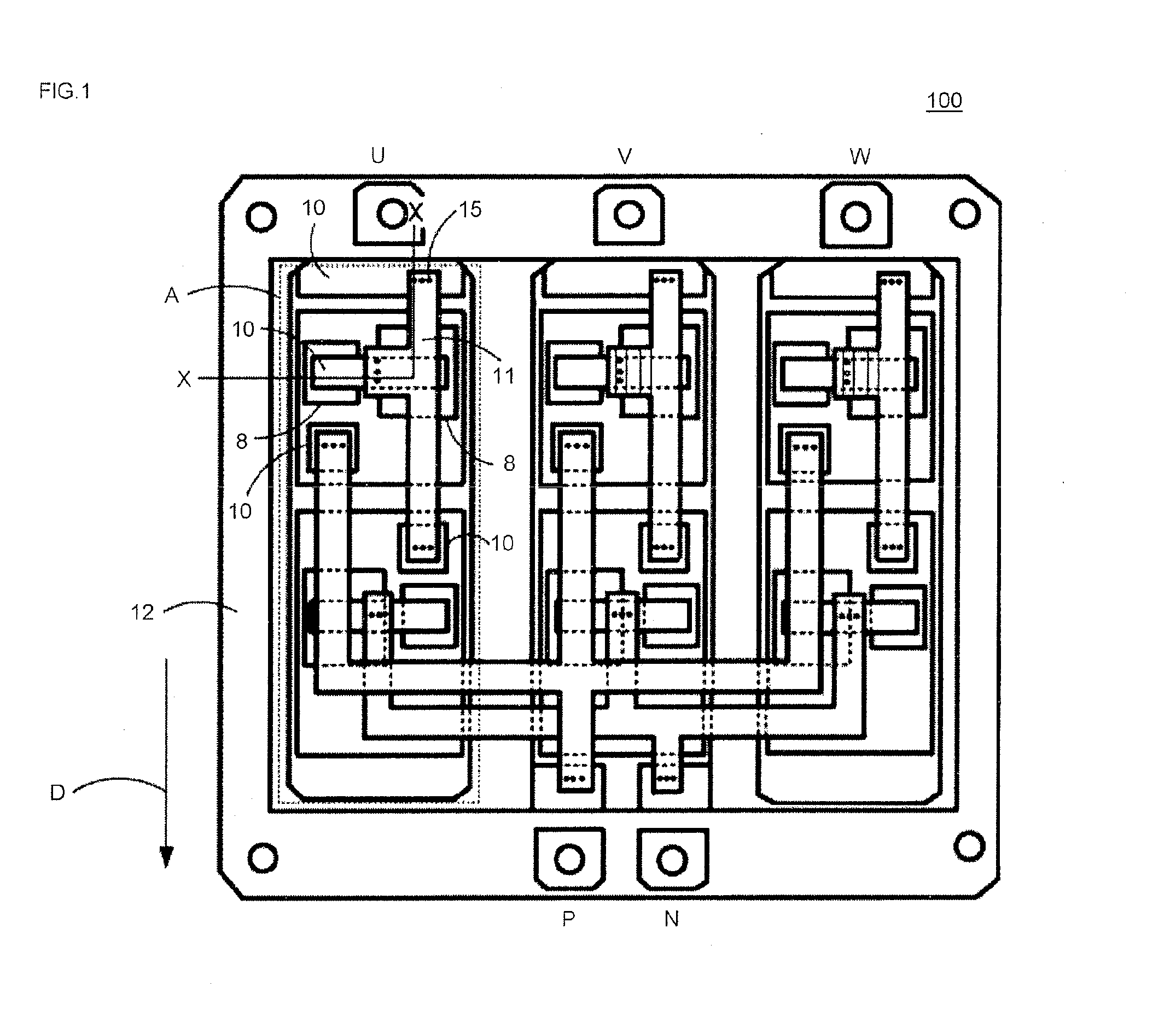
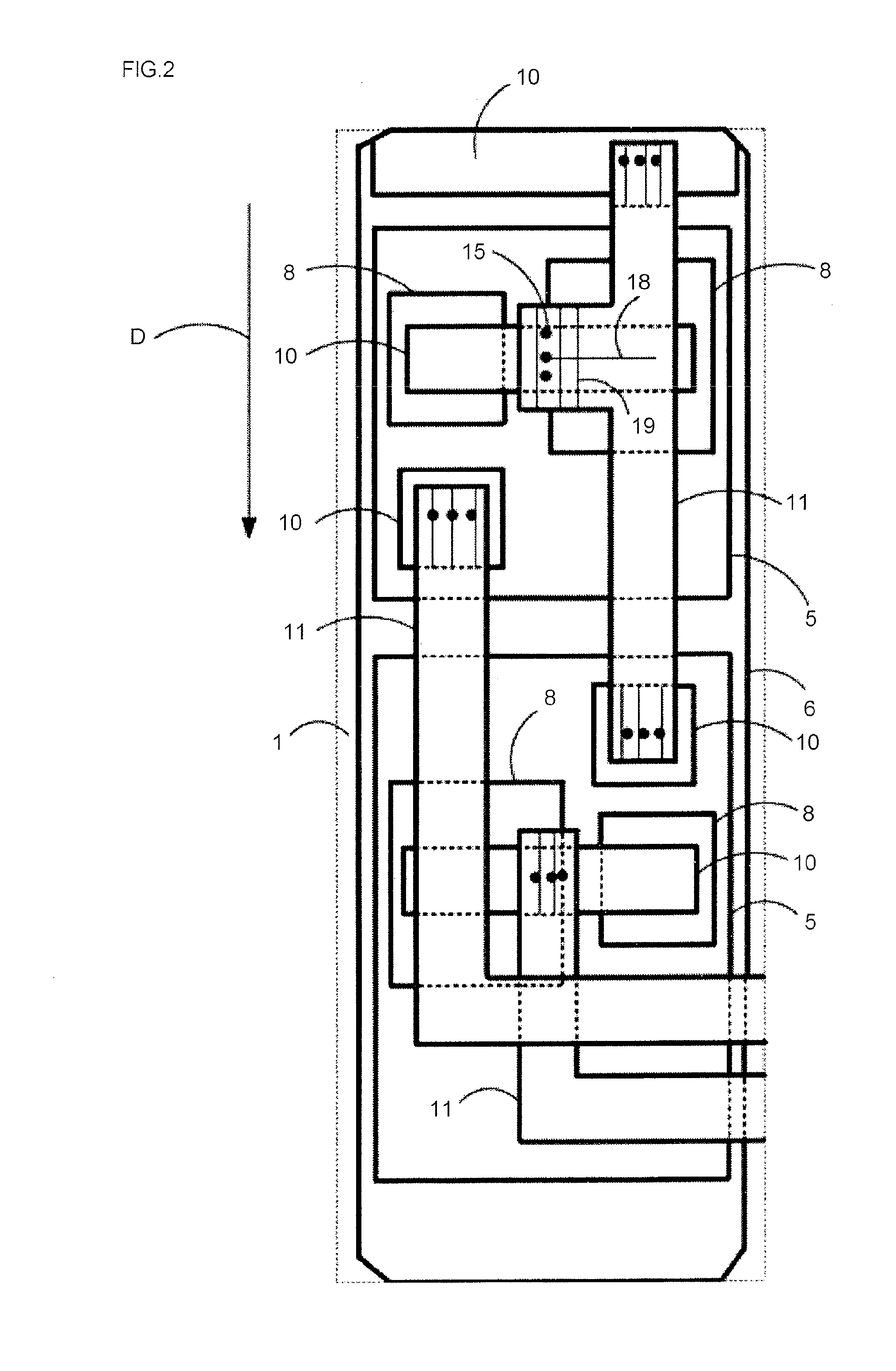
[0047]FIGS. 1 to 3 are configuration diagrams of a semiconductor device according to the first embodiment of the present invention. FIG. 1 is a plan view showing substantial parts, FIG. 2 is an enlarged view of a section A shown in FIG. 1, and FIG. 3 is a schematic cross-sectional view of the substantial parts, taken from line X-X of FIG. 1. A semiconductor device 100 shown in FIG. 1 is same as the power semiconductor module 500 shown in FIG. 11. In FIG. 1, three identical sections including the section A are arranged side by side, and rolling traces 19 (same as the rolling traces 69 of the power semiconductor module 500) of all lead frames are arranged in the direction of the arrow D. The direction of the arrow D corresponds to the rolling direction, the direction of the rolling traces 19.
[0048]The semiconductor device 100 is configured by a heat dissipating base 1, a patterned insulating substrate 6 attached to the heat dissipating base 1 with a solder 2 therebetween, and a semico...
second embodiment
[0066]FIGS. 6 to 10 are process diagrams showing a method of manufacturing a semiconductor device according to the second embodiment of the present invention, the process diagrams being cross-sectional diagrams showing steps of manufacturing substantial parts of the semiconductor device.
[0067]In FIG. 6, upper lead frames 11 are cut out of a rolled copper plate 21. In doing so, the places to dispose the upper lead frames 11 in the semiconductor device 100 (power semiconductor module) are predicted, and all of the upper lead frames 11 (the section A is shown) are cut out in such a manner that the rolling traces 19 are arranged in the same direction D (the rolling direction).
[0068]Next, lower lead frames 10 are disposed on a front surface electrode of the semiconductor chips 8. The rolling direction of the lower lead frames 10 may or may not have to be the same as that of the upper lead frames 11 and can be any direction.
[0069]Subsequently, the upper lead frames 11 are disposed on the ...
PUM
| Property | Measurement | Unit |
|---|---|---|
| angle | aaaaa | aaaaa |
| thickness | aaaaa | aaaaa |
| conductive | aaaaa | aaaaa |
Abstract
Description
Claims
Application Information