Apparatus for manufacturing polysilicon based electron-beam melting using dummy bar and method of manufacturing polysilicon using the same

a technology of electron beam and manufacturing method, which is applied in the direction of glass rolling apparatus, manufacturing tools, and compounds, etc., can solve the problems of low production efficiency, large amount of contaminants generated by the production process, and the production process is not suited to the production of semiconductor level silicon, so as to improve the efficiency of silicon refining and high purity

Active Publication Date: 2013-11-07
KOREA INST OF ENERGY RES
View PDF9 Cites 5 Cited by
  • Summary
  • Abstract
  • Description
  • Claims
  • Application Information

AI Technical Summary

Benefits of technology

[0011]The present invention provides an apparatus for manufacturing high purity polysilicon based on electron-beam melting using a dummy bar to improve silicon refining efficiency.

Problems solved by technology

However, such a silicon production process generates a large amount of contaminants, and has low production efficiency in spite of high production cost.
Thus, the silicon production process is not suited to production of semiconductor level silicon used as a raw material for photovoltaic cells, and efforts for developing metallurgical refining processes capable of achieving mass production of high purity silicon at low cost have been actively attempted.

Method used


Image

  • Apparatus for manufacturing polysilicon based electron-beam melting using dummy bar and method of manufacturing polysilicon using the same
  • Apparatus for manufacturing polysilicon based electron-beam melting using dummy bar and method of manufacturing polysilicon using the same
  • Apparatus for manufacturing polysilicon based electron-beam melting using dummy bar and method of manufacturing polysilicon using the same

Examples


example

[0069]Next, the constitution and functions of the present invention will be explained in more detail with reference to the following examples. These examples are provided for illustrative purposes only and are not to be in any way construed as limiting the invention.

[0070]A description of details apparent to those skilled in the art will be omitted herein.

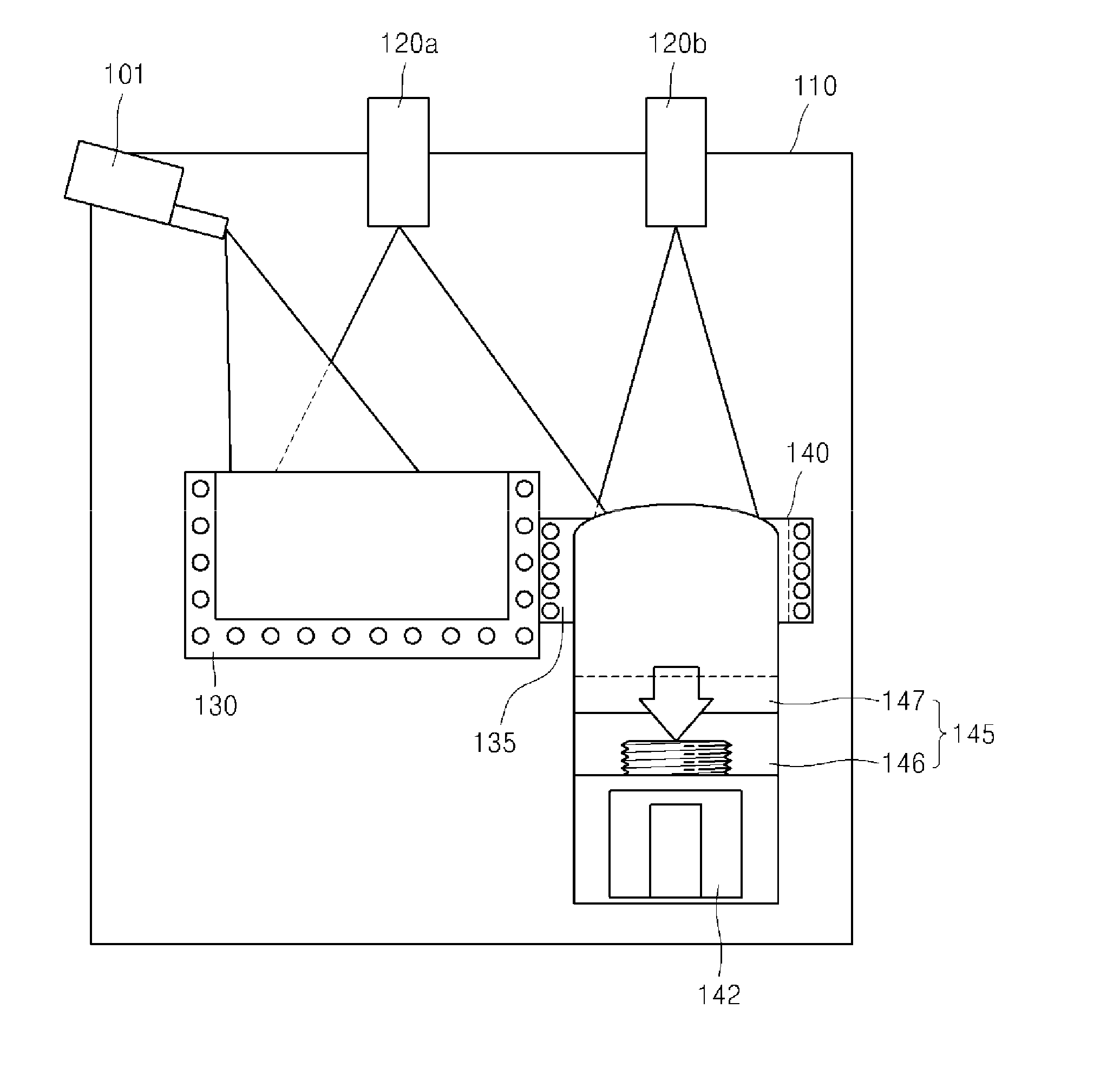
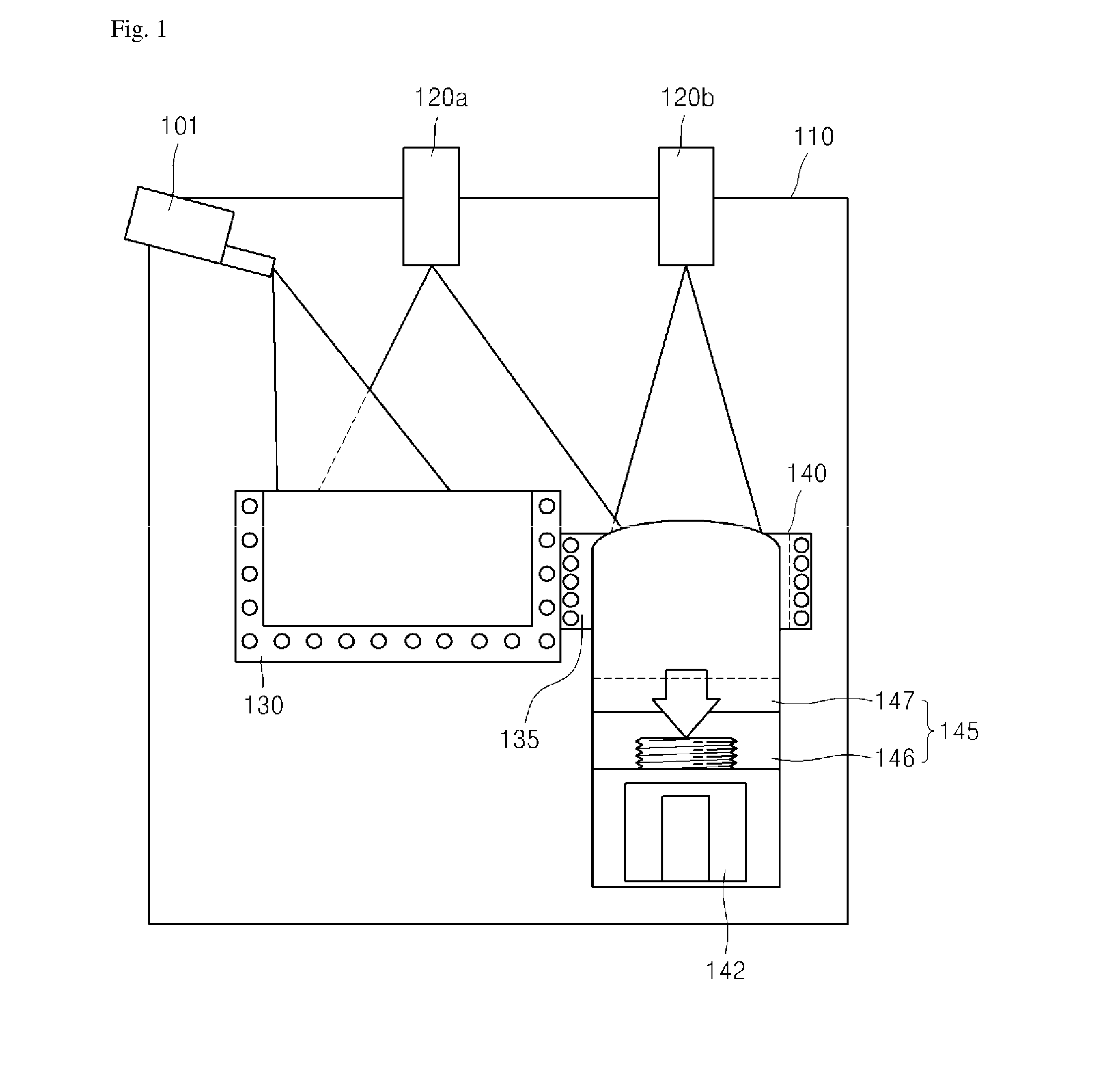
[0071]First, polysilicon was produced by the following process.

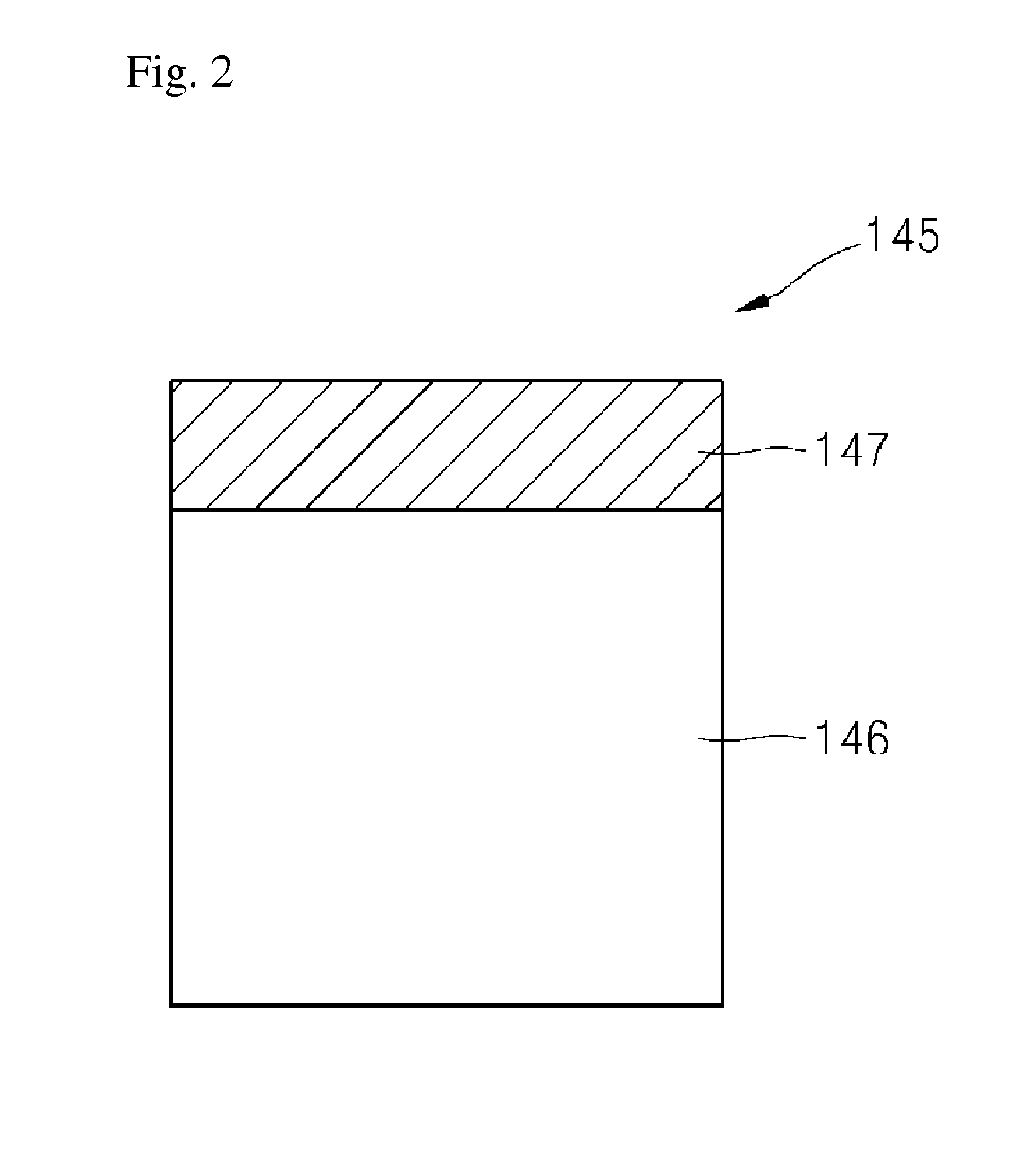
[0072]A graphite dummy bar was mounted inside the unidirectional solidification unit and a silicon chunk having a purity of 9N and a weight of 180 g was fed thereto. Then, with the vacuum chamber maintained under a high vacuum of 10-5 Torr, an electron beam was irradiated from the second electron gun to the silicon at an output energy of 2000 kW / m2 for 10 minutes to melt the raw silicon, and the molten silicon was joined to the dummy bar under the molten silicon.

[0073]Silicon powder having a particle size of 1 to 10 mm and fed to the water cooling type crucible through ...


PUM

PropertyMeasurementUnit
thicknessaaaaaaaaaa
mean particle diameteraaaaaaaaaa
internal pressureaaaaaaaaaa

Abstract

Methods and apparatus for manufacturing high purity polysilicon. The apparatus includes a vacuum chamber; first and second electron guns disposed at an upper side of the vacuum chamber to irradiate electron beams into the vacuum chamber; a silicon melting unit which is placed on a first electron beam-irradiating region corresponding to the first electron gun and to which powdery raw silicon is fed and melted by the first electron beam; and a unidirectional solidification unit placed on a second electron beam-irradiating region corresponding to the second electron gun. The unidirectional solidification unit is provided therein with a start block driven in a downward direction to transfer molten silicon in the downward direction and is formed at a lower side thereof with a cooling channel. The start block includes a dummy bar having a silicon button joined to an upper portion of the dummy bar.

Description

BACKGROUND[0001]1. Technical Field[0002]The present invention relates to a technique for manufacturing polysilicon, and more particularly, to a method and apparatus for manufacturing polysilicon based on electron-beam melting using a dummy bar to improve silicon refining efficiency.[0003]2. Description of the Related Art[0004]Purity of silicon is typically represented by 2N, 3N, 6N, 11N, and the like. Here, the numeral in front of ‘N’ means the number of nines (9) in percent by weight (wt %). For example, 2N means a purity of 99%, 6N means a purity of 99.9999%, and 11N means a purity of 99.999999999%.[0005]Semiconductor level silicon requires an ultra-high purity approaching 11N. However, as known in the art, silicon used as a raw material for photovoltaic cells and having a relatively low purity of 5N to 7N provides similar optical conversion efficiency to silicon having a high purity of 11N.[0006]Semiconductor level silicon is produced through chemical gasification processes. Howe...

Claims


Application Information

Patent Timeline
Patent Type & Authority Applications(United States)
IPC IPC(8): C01B33/02B01J19/08C01B33/037
CPCB01J6/007B01J19/085B01J2219/00135C01B33/037C30B13/22
Inventor JANG, BO YUNLEE, JIN SEOKKIM, JOON SOOAHN, YOUNG SOO
Owner KOREA INST OF ENERGY RES
Why Eureka
Try Eureka