

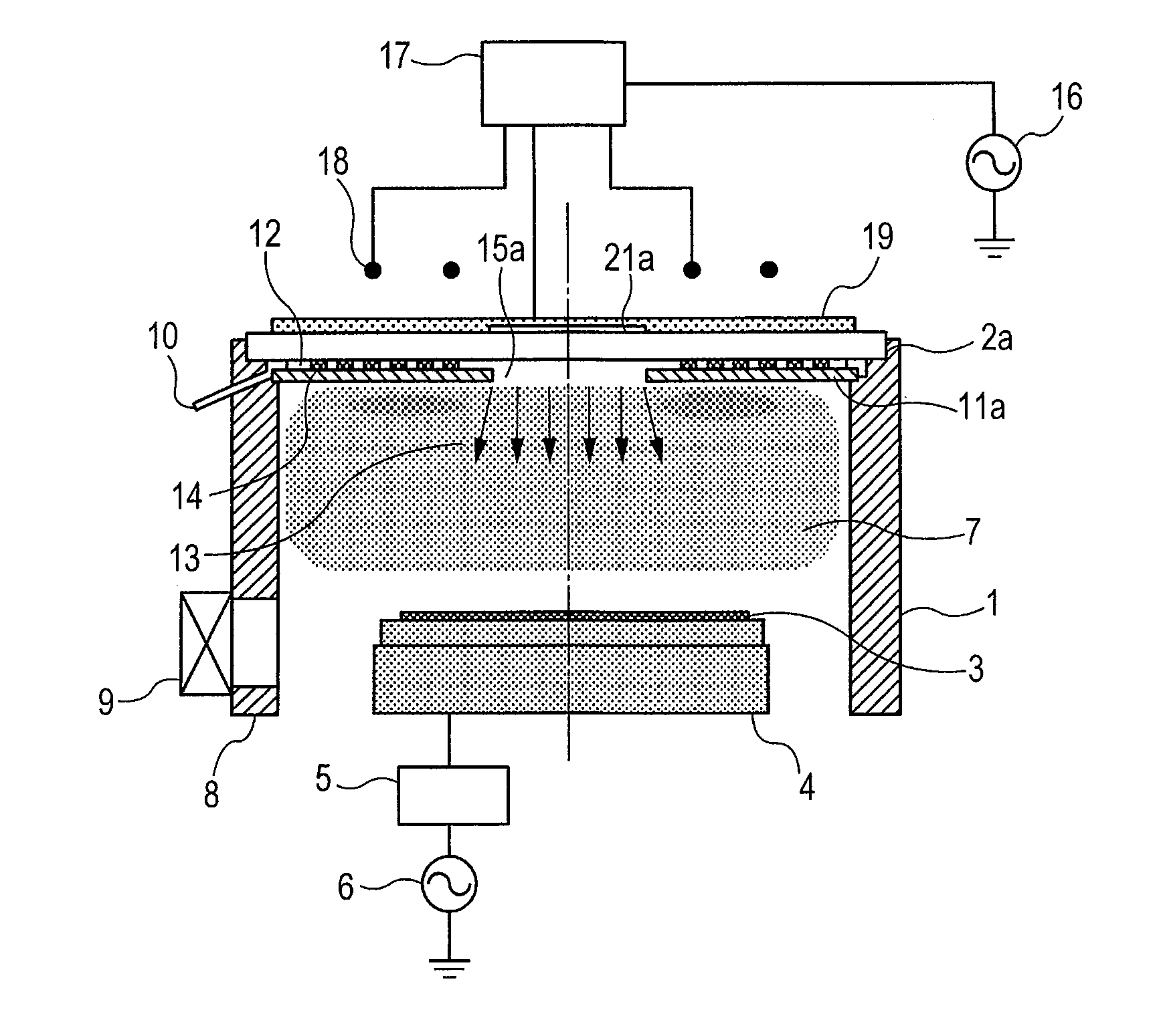
Plasma processing apparatus
a processing apparatus and plasma technology, applied in the direction of electrical apparatus, plasma technique, electric discharge tube, etc., can solve the problems of deterioration in the etching rate, affecting the processing efficiency, and affecting the production efficiency of the reaction product, so as to reduce the generation of foreign substances or adhesion of reaction products, the effect of high etching performance and mass production stability
- Summary
- Abstract
- Description
- Claims
- Application Information
AI Technical Summary
Benefits of technology
Problems solved by technology
Method used
Image

Examples
second embodiment
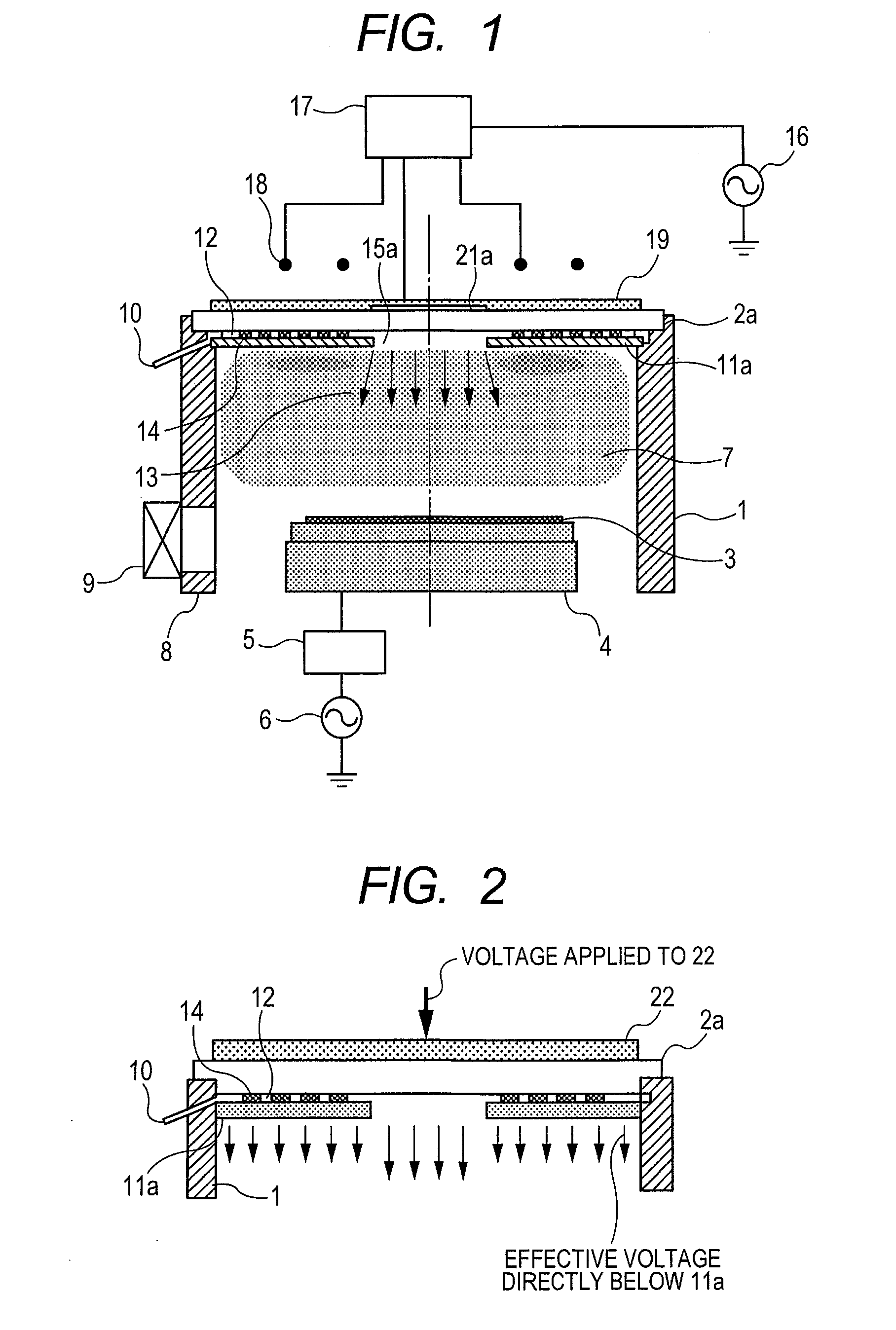
[0049]A plasma processing apparatus according to a second embodiment of the present invention will be described referring to FIGS. 4 to 10. Referring to FIG. 4, the same reference numerals as those shown in FIG. 1 denote the same members, and redundant explanations will be omitted. This drawing is different from FIG. 1 in that the lower surface of the center of the dielectric vacuum window 2b has a convex shape which is fitted with the center opening of the gas release plate 11b so as to leave a predetermined gap to form a slit 15b as a gas outlet. A reference numeral 21b denotes a notch.
[0050]The process gas 13 is released from the slit 15b in the circumference direction formed between a circular trapezoidal protrusion formed on the center part of the dielectric vacuum window 2b and the circular opening in the center part of the gas release plate 11b.
[0051]FIG. 5 is a detailed view showing a peripheral part of the faraday shield 19 of the plasma processing apparatus according to t...
third embodiment
[0061]A third embodiment of the present invention will be described referring to FIG. 9. FIG. 9 is a detailed view of another embodiment of a peripheral part of the faraday shield of the plasma processing apparatus according to the second embodiment. Referring to FIG. 9, the same reference numerals as those described in the embodiment denote the same members, and redundant explanations will be omitted. This embodiment is different from the one shown in FIG. 5 in that the method of supplying gas to the dielectric vacuum window 2 and the gas release plate 11 is different from the method of supplying gas to the high dielectric bodies 14. A faraday shield 28 has a gas flow passage configuration that is the same as the gas flow passage 29 formed in a high dielectric body 27, in other words, the configuration which includes a plurality of flow passages radially connected to the outer peripheral part from the center opening hole in this case. A notch 30 with the same configuration as the g...
fourth embodiment
[0063]A fourth embodiment of the present invention will be described referring to FIG. 10.
[0064]FIG. 10 is a detailed view of another embodiment of a peripheral part of the faraday shield of the plasma processing apparatus according to the second embodiment. The reference numerals shown in FIG. 9 which are the same as those described in the aforementioned embodiment denote the same members, and redundant explanations will be omitted. This embodiment is different from the one shown in FIG. 9 in that a low dielectric body 31 with permittivity lower than that of the dielectric vacuum window 25 and the gas release plate 26 (for example, polytetrafluoroethylene) is provided instead of the air layer of the notch 30 formed in the faraday shield 28. The semiconductor substrate is machined using the inductively coupled plasma processing apparatus shown in FIG. 4, which is provided with the low dielectric body 31 with low permittivity as shown in FIG. 10. This makes it possible to perform pla...
PUM
| Property | Measurement | Unit |
|---|---|---|
| thickness | aaaaa | aaaaa |
| size | aaaaa | aaaaa |
| frequency | aaaaa | aaaaa |
Abstract
Description
Claims
Application Information