Display Device and Method for Manufacturing the Same

Inactive Publication Date: 2013-11-14
SEMICON ENERGY LAB CO LTD
View PDF4 Cites 34 Cited by
  • Summary
  • Abstract
  • Description
  • Claims
  • Application Information

AI Technical Summary

Benefits of technology

[0036]Furthermore, in the above structure, a fourth electrode formed of the same material as the first electrode of the light-emitting element is further included. The fourth electrode is electrically connected to a terminal electrode. The auxiliary electrode is provided on and in contact with the fourth electrode. The second electrode of the light-emitting element is provided on and in contact with the fourth electrode. That is to say, in the display device, the auxiliary electrode is connected to a wiring in a lower layer at a portion different from a portion where the auxiliary electrode is connected to a wiring in an upper layer. Specifically, in the pixel portion, to improve an aperture ratio, the auxiliary electrode is preferably in contact with the se

Problems solved by technology

However, with the use of the material, film resistance is easily increased and a nonuniform potential distribution occ

Method used


Image

  • Display Device and Method for Manufacturing the Same
  • Display Device and Method for Manufacturing the Same
  • Display Device and Method for Manufacturing the Same

Examples


embodiment 1

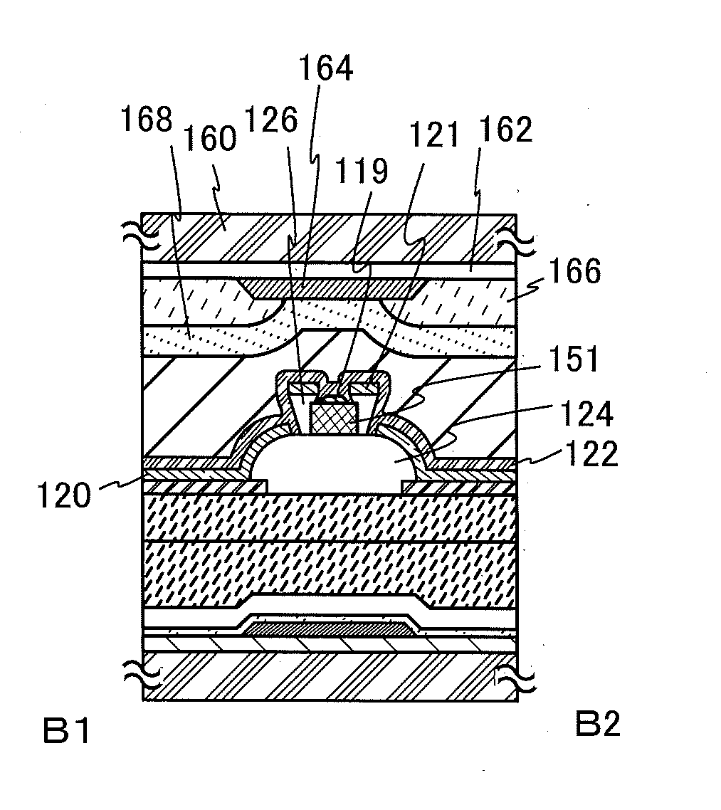
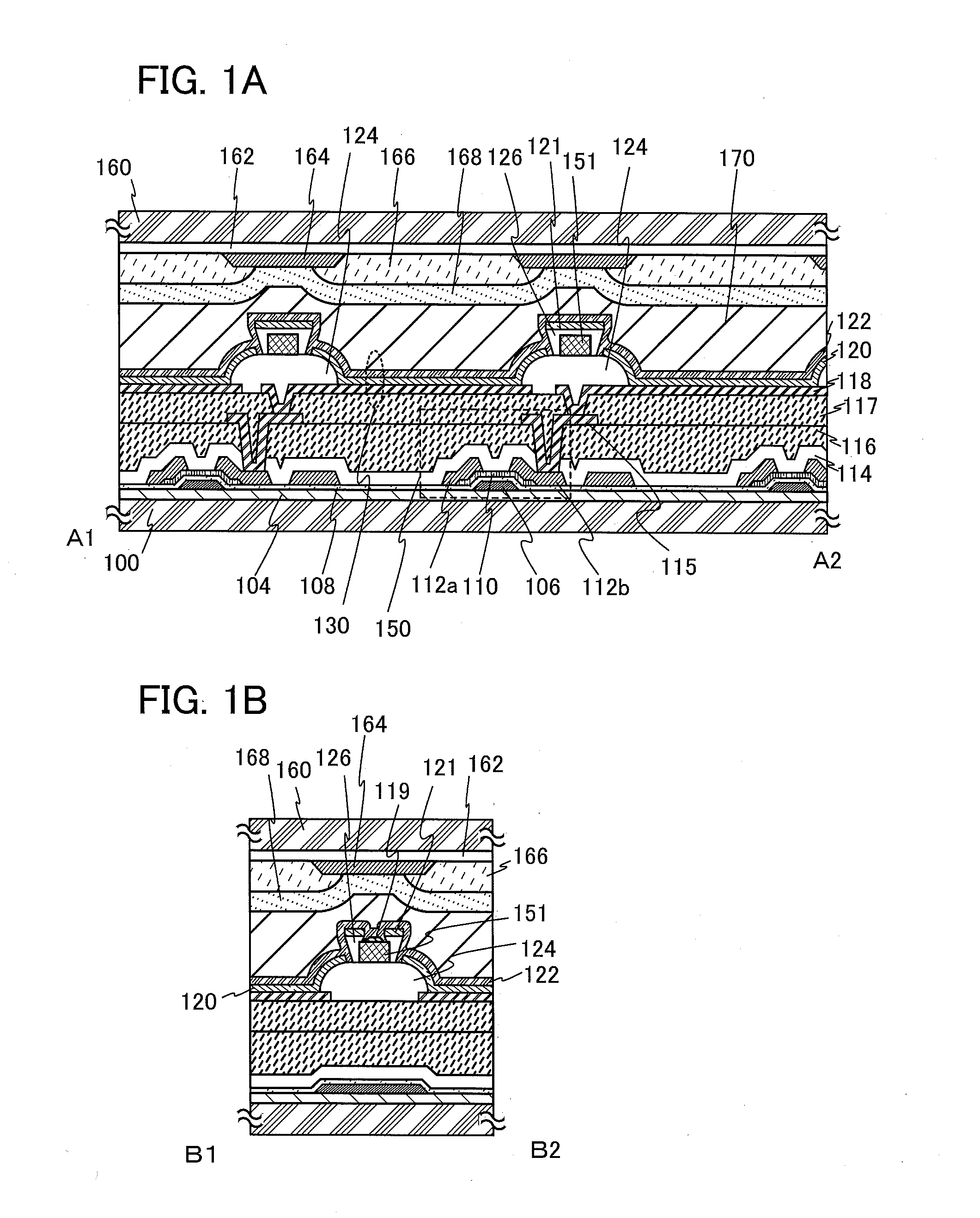
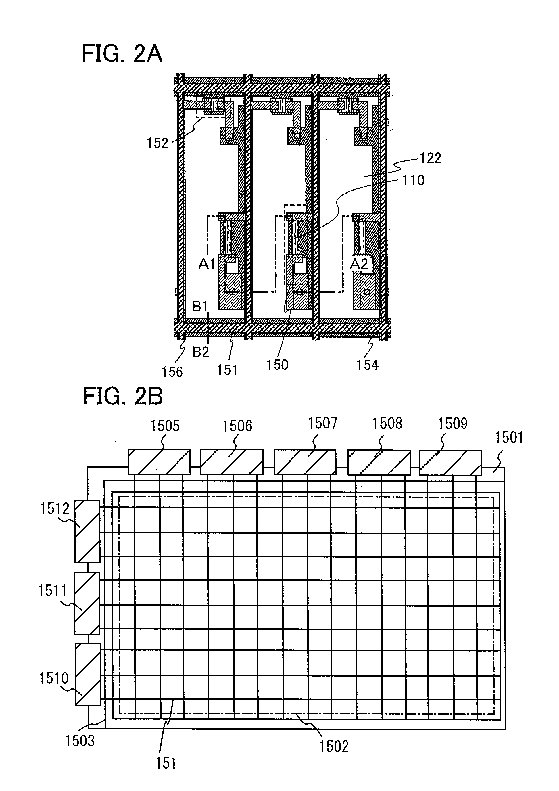
[0043]In this embodiment, a structure of a display device which is one embodiment of the present invention is described with reference to FIGS. 1A and 1B, FIGS. 2A and 2B, and FIGS. 3A and 3B.

[0044]FIG. 2B is a general schematic view of the display device. The display device in FIG. 2B includes a pixel portion 1502 including a plurality of light-emitting elements over a substrate 1501 having an insulating surface. A sealing substrate 1503 including a color filter and the substrate 1501 are fixed so that the color filter overlaps with the pixel portion 1502. Terminals connected to the outside of the display device are connected to FPCs 1505, 1506, 1507, 1508, 1509, 1510, 1511, and 1512. Note that the sealing substrate 1503 does not overlap with the terminals connected to the FPCs. FIG. 2B illustrates an example of providing an auxiliary electrode 151 with a net-like shape. The potential of the auxiliary electrode 151 is set to a fixed potential or a ground potential through the FPCs....

embodiment 2

[0113]A display device disclosed in this specification can be applied to a variety of electronic appliances (including game machines). Examples of the electronic appliances include a television device (also referred to as a television or a television receiver), a monitor of a computer, cameras such as a digital camera and a digital video camera, a digital photo frame, a mobile phone, a portable game machine, a portable information terminal, an audio reproducing device, a game machine (e.g., a pachinko machine or a slot machine), and a game machine console. Specific examples of the electronic appliances are illustrated in FIGS. 4A and 4B.

[0114]FIG. 4A illustrates a table 9000 having a display portion. In the table 9000, a display portion 9003 is incorporated in a housing 9001. A display device manufactured with the use of one embodiment of the present invention can be used for the display portion 9003, and an image can be displayed on the display portion 9003. Note that the housing 9...


PUM


Abstract

A structure of an EL display device which has an increased display area is provided. Further, a structure of an EL display device which has a high definition display is provided. An auxiliary electrode is formed over a first partition and side surfaces of the auxiliary electrode are covered with a second partition. A top surface of the auxiliary electrode is in contact with the conductive film which is one electrode of a light-emitting element and has a light-transmitting property, which enables a large-area display. Further, even the distance between the adjacent light-emitting elements is shortened, the auxiliary electrode can be provided between the adjacent light-emitting elements, which enables a high definition display.

Description

BACKGROUND OF THE INVENTION[0001]1. Field of the Invention[0002]The present invention relates to a display device, a method for manufacturing the display device, and an electronic appliance including the display device.[0003]In this specification, a semiconductor device generally means a device which can function by utilizing semiconductor characteristics, and an electrooptic device, a semiconductor circuit, and an electronic appliance are all semiconductor devices.[0004]2. Description of the Related Art[0005]A transistor formed over a glass substrate or the like includes amorphous silicon, polycrystalline silicon, or the like, as typically seen in a liquid crystal display device or an EL display device. Although a transistor using amorphous silicon has low field effect mobility, it can be formed over a larger glass substrate. On the other hand, although a transistor using polycrystalline silicon has high field effect mobility, it is not suitable for being formed over a larger glass...

Claims


Application Information

Patent Timeline
IPC IPC(8): H01L27/32H05B44/00
CPCH01L27/3279H01L27/1225H10K59/38H10K59/1315H10K59/122H10K50/824H10K50/828H01L29/7869H10K59/32H10K59/125H10K50/11H10K50/805H10K59/123
Inventor HIRAKATA, YOSHIHARUYAMAZAKI, SHUNPEIKUWABARA, HIDEAKI
Owner SEMICON ENERGY LAB CO LTD
Why Eureka
Try Eureka