Semiconductor device and a method for manufacturing the same

a technology of semiconductor devices and semiconductors, applied in the direction of semiconductor devices, basic electric elements, electrical equipment, etc., can solve the problems of reducing driving capability and the bottleneck in the cutting cost of only reducing the feature size, so as to improve the mobility of the charge carrier of the semiconductor device, prevent the stress from decreasing, and enhance the driving capability of the device

Inactive Publication Date: 2013-11-28
INST OF MICROELECTRONICS CHINESE ACAD OF SCI
View PDF4 Cites 10 Cited by
  • Summary
  • Abstract
  • Description
  • Claims
  • Application Information

AI Technical Summary

Benefits of technology

[0030]The present invention inserts a liner layer having an identical or similar material to the stress layer of the source / drain region between the STI and the stress layer of the source / drain region as a crystal seed layer or nucleating layer for epitaxial growth, thereby eliminating the STI edge effect, i,e., eliminating the gap between the STI and the stress layer of the source / drain region, preventing the stress from decreasing, and improving the charge carrier mobility of the MOS device so as to enhance the driving capability of the device,

Problems solved by technology

The method of cutting cost by only reducing the feature size has encountered a bottleneck, especially when the feature size decreases to less than 150 nm.
Similar to PMOSs, SiC will also get thinner at the STI edge of NMOSs, thereby reducing driving capability.

Method used


Image

  • Semiconductor device and a method for manufacturing the same
  • Semiconductor device and a method for manufacturing the same
  • Semiconductor device and a method for manufacturing the same

Examples


embodiments

[0034]Characteristics and technical effects of the technical solution of the present invention will be described in detail with reference to figures and in combination with illustrative embodiments. What needs to be noted is that similar reference signs refer to similar structures, but the terms “first”, “second”, “above”,“below”, “thick” and “thin” used in the present application can be used for modifying structures and method steps of various devices. These modifications, unless particularly described, do not indicate the space, order, or hierarchical relationship of the structures and method steps of the devices modified.

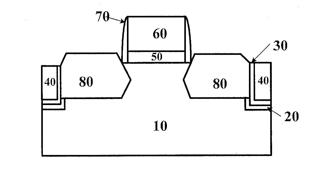
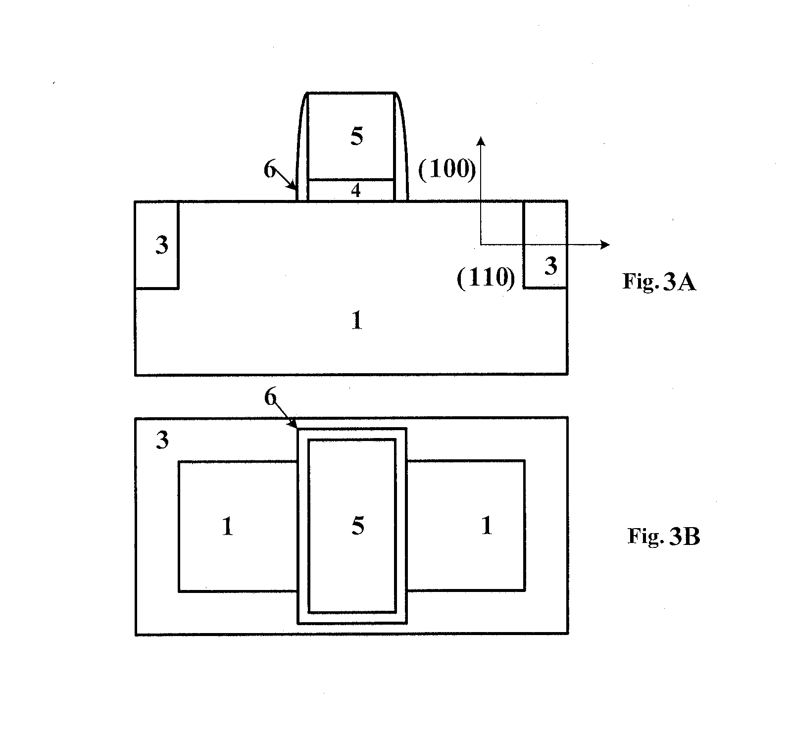
[0035]FIGS. 7A to 13C show cross-sectional views of SiGe that is epitaxially grown on the source / drain region in accordance with the present invention.

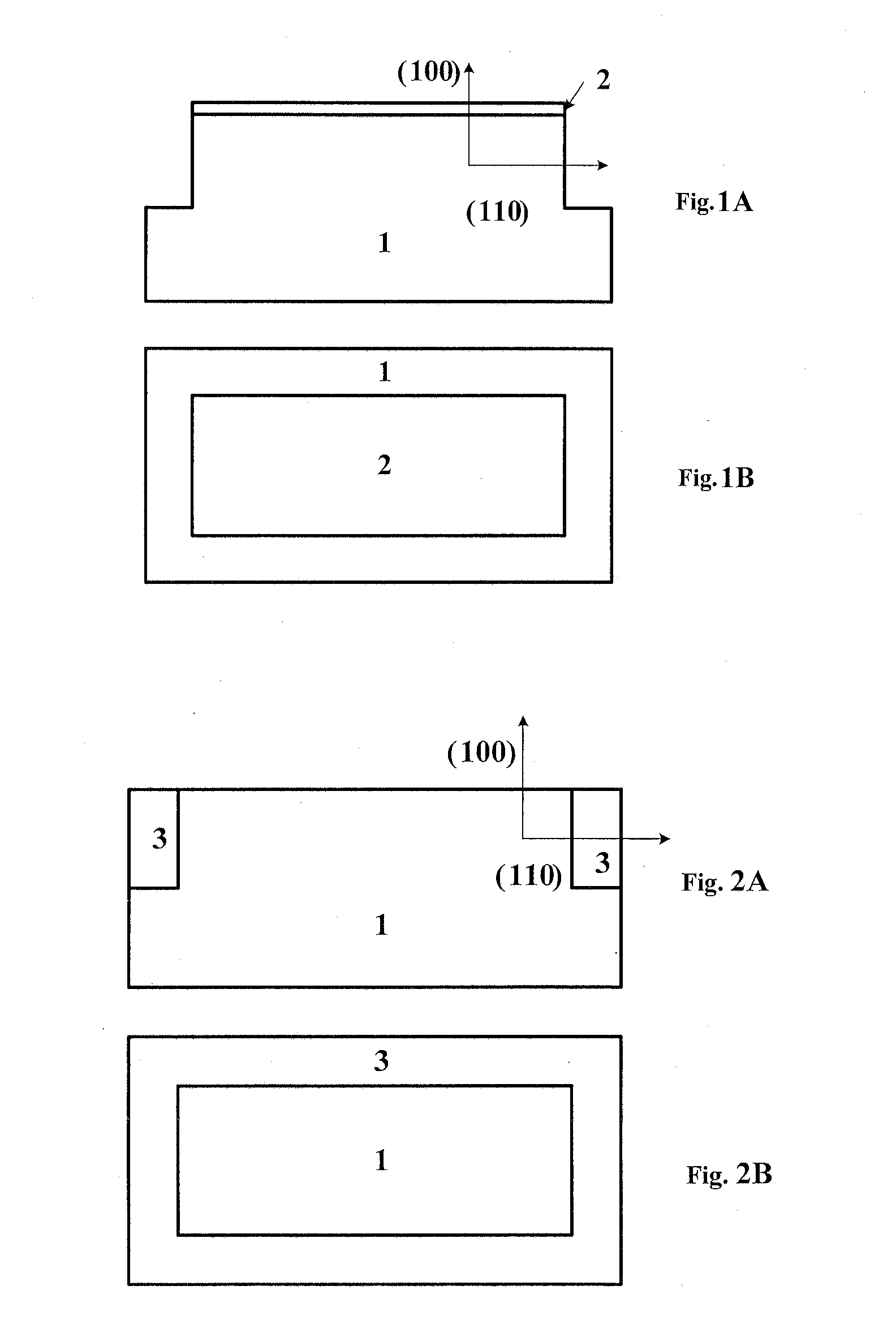
[0036]First, as shown in FIGS. 7A and 7B, a shallow trench surrounding one opening region (or an active region) is formed by etching the substrate 10 through conventional mask exposure, and then a pad oxide layer 2...


PUM


Abstract

A semiconductor device comprises a substrate; a shallow trench isolation embedded in the substrate and forms at least one opening region; a channel region located in the opening region; a gate stack including a gate dielectric layer and a gate electrode layer, located above said channel region; a source/drain region located on both sides of the channel region, including a stress layer which provides strain for the channel region. A liner layer is provided between the shallow trench isolation and the stress layer, which serves as a crystal seed layer of the stress layer. A liner layer and a pad oxide layer are provided between the substrate and the shallow trench isolation. The liner layer is inserted between the STI and the stress layer of the source/drain region as a crystal seed layer or nucleating layer for epitaxial growth, thereby eliminating the STI edge effect during the source/drain strain engineering.

Description

CROSS-REFERENCE TO RELATED PATENT APPLICATIONS[0001]This application is a U.S. National Phase Application under 35 U.S.C. §371 of International Patent Application No. PCT / CN2012 / 078780, filed Jul. 18, 2012, and claims the benefit of Chinese Patent Application No. 201210162593.2, filed on May 23, 2012, titled “SEMICONDUCTOR DEVICE AND A METHOD FOR MANUFACTURING THE SAME,” all of which are incorporated by reference herein in its entirety.FIELD OF THE INVENTION[0002]The present invention relates to a field of semiconductor devices. In particular, the present invention relates to a semiconductor device structure with an improved epitaxial edge and a method for manufacturing the same.BACKGROUND OF THE INVENTION[0003]The method of cutting cost by only reducing the feature size has encountered a bottleneck, especially when the feature size decreases to less than 150 nm. In such a case, many physical parameters can not change in proportion, such as silicon band gap Eg, Fermi potential ωF, i...

Claims


Application Information

Patent Timeline
Patent Type & Authority Applications(United States)
IPC IPC(8): H01L29/78H01L29/66
CPCH01L29/7846H01L29/66553H01L29/045H01L29/66636
Inventor WANG, GUILEICUI, HUSHANZHAO, CHAO
Owner INST OF MICROELECTRONICS CHINESE ACAD OF SCI
Why Eureka
Try Eureka