Method for driving memory element

a memory element and memory technology, applied in the field of memory elements, can solve the problems of unsuitable signal processing circuits, achieve the effect of reducing the power consumption of a semiconductor device using the memory element, high speed, and reducing the power consumption of a short tim

Active Publication Date: 2013-11-28
SEMICON ENERGY LAB CO LTD
View PDF2 Cites 15 Cited by
  • Summary
  • Abstract
  • Description
  • Claims
  • Application Information

AI Technical Summary

Benefits of technology

[0027]In addition, in a memory element according to one embodiment of the present invention, an operation for stopping supply of power and an operation for resuming supply of power are performed at high speed; therefore, stop of supply of power for a short time can be easily performed. As a result, power consumption of a semiconductor device using the memory element can be efficiently reduced.
[0028]According to one embodiment of the present invention, a memory element which can keep a stored logic state even when the supply of power is stopped or a memory device using the memory element can be provided.
[0029]According to one embodiment of the present invention, a driving method for increasing the speed of an operation of stopping supply of power to the memory element can be provided. Further, a driving method for increasing the speed of an operation of resuming supply of power to the memory element can be provided. As a result, a memory element which facilitates stop of supply of power for a short time or a memory device using the memory element can be provided.
[0030]A semiconductor device having reduced power consumption by using the memory element or the memory device can be provided.

Problems solved by technology

Therefore, such a signal processing circuit is not suitable in the case where the power supply is stopped for a short time so as to reduce power consumption.

Method used


Image

  • Method for driving memory element
  • Method for driving memory element
  • Method for driving memory element

Examples


embodiment 1

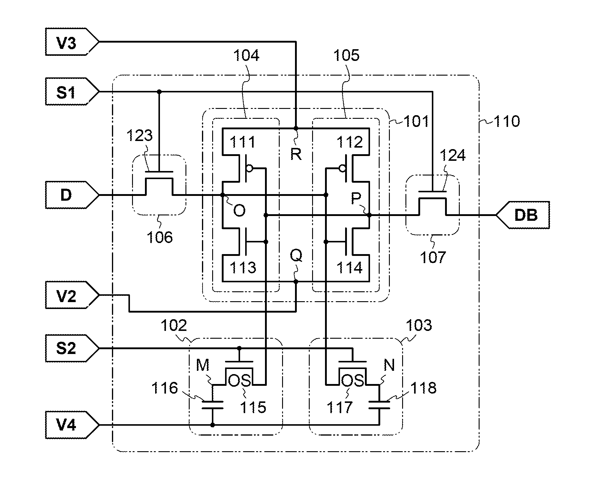
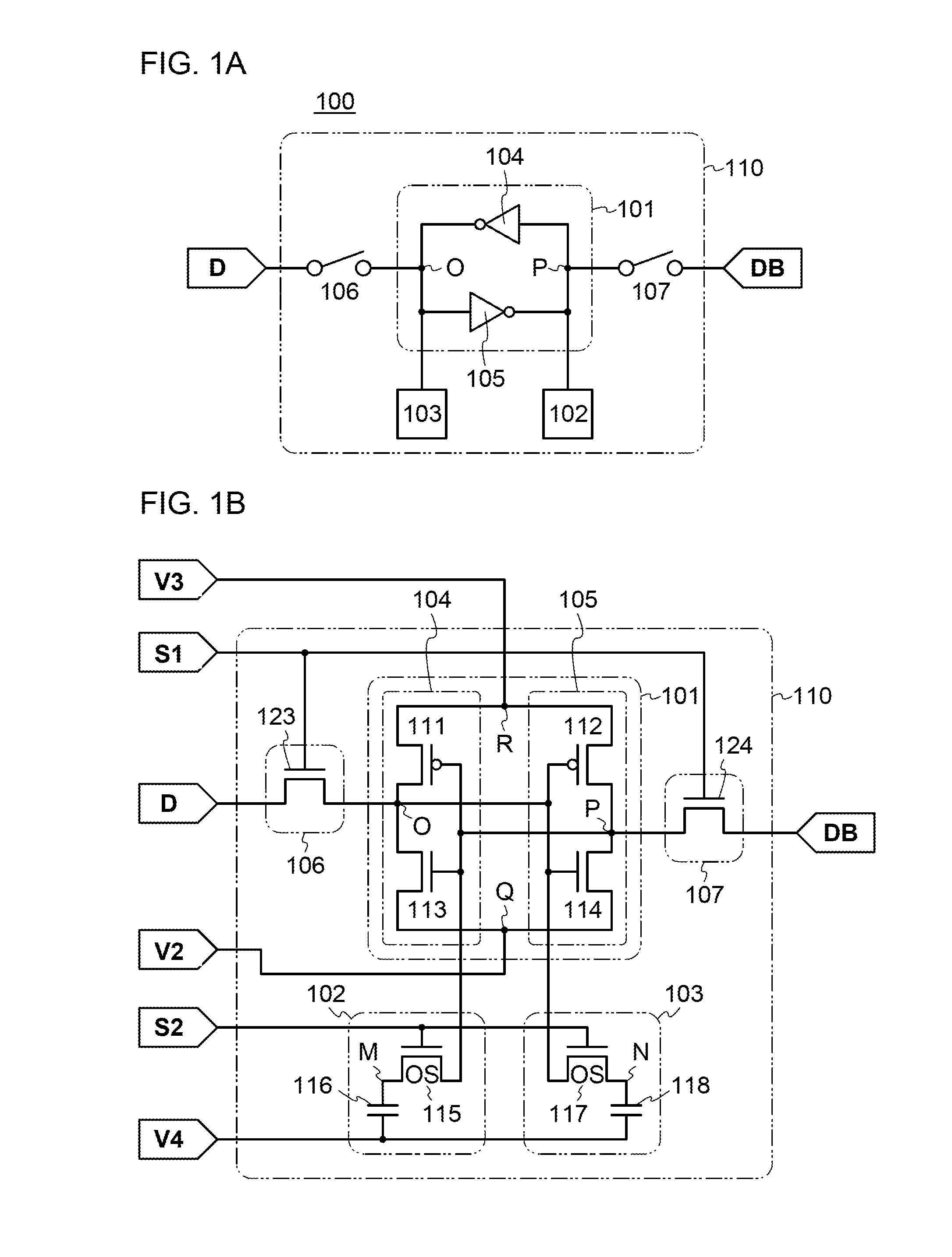
[0051]A memory element 110 according to one embodiment of the present invention will be described with reference to FIGS. 1A and 1B. FIGS. 1A and 1B are circuit diagrams showing the circuit configuration of the memory element 110. In FIG. 1A, part of the circuit configuration in FIG. 1B is replaced with logic symbols. Note that in each of circuit diagrams, in some cases, “OS” (abbreviation of an oxide semiconductor) is written besides a transistor in order to indicate that the transistor includes an oxide semiconductor.

[0052]The memory element 110 illustrated in FIGS. 1A and 1B includes a logic circuit 101, a memory circuit 102, a memory circuit 103, a switch 106, and a switch 107. Further, the logic circuit 101 includes a first inverter circuit 104 and a second inverter circuit 105. The first inverter circuit 104 includes a p-channel transistor 111 and an n-channel transistor 113. The second inverter circuit 105 includes a p-channel transistor 112 and an n-channel transistor 114.

[0...

embodiment 2

[0132]In this embodiment, an example where a memory cell array is formed to include the plurality of memory elements 110 illustrated in FIGS. 1A and 1B will be described with reference to FIG. 6 and FIG. 7. FIG. 6 is an example of a block diagram of a semiconductor device including (m×n) memory elements 110.

[0133]A memory device 200 illustrated in FIG. 6 includes m signal lines SL1 (m is an integer of 2 or more), m signal lines SL2, n bit lines BL (n is an integer of 2 or more), n inverted bit lines BLB, a first wiring 221 (not illustrated), a second wiring 222, a third wiring 223, m fourth wirings 224, a memory cell array 210 having the memory elements 110 arranged in matrix of m rows (in the vertical direction)×n columns (in the horizontal direction), a first driver circuit 211, and a second driver circuit 212. The first driver circuit 211 is connected to the n bit lines BL and the n inverted bit lines BLB. The second driver circuit 212 is connected to the m signal lines SL1, the ...

embodiment 3

[0141]In this embodiment, an example of a method for manufacturing the memory element described in Embodiment 1 will be described with reference to FIGS. 8A to 8E, FIGS. 9A to 9D, FIGS. 10A to 10D, and FIGS. 11A and 11B. First, a method for manufacturing a transistor in a lower portion of the memory device will be described, and then, a method for manufacturing a transistor and a capacitor in an upper portion of the memory device will be described. Note that in cross-sectional views illustrating a manufacturing process, A1-A2 is a cross section illustrating a manufacturing step of an n-channel transistor and B1-B2 is a cross section illustrating a manufacturing step of a p-channel transistor.

[0142]First, a substrate 300 over which a semiconductor layer 304 is provided with an insulating layer 302 laid therebetween is prepared (see FIG. 8A).

[0143]Examples of the substrate 300 include a single crystal semiconductor substrate of silicon, silicon carbide, or the like, a polycrystalline ...


PUM


Abstract

To provide a memory element which keeps a stored logic state even without supply of power. To increase an effect of reducing power consumption by facilitating stop of supply of power to the memory element for a short time. Data (potential) held in a node in a logic circuit can be swiftly saved on a node where one of a source and a drain of the transistor and one electrode of the capacitor included in a memory circuit are connected by lowering a potential of the other electrode of a capacitor before a transistor is turned on. By making a potential of the other electrode of the capacitor when the transistor is in an off state higher than a potential of the other electrode of the capacitor when the transistor is in an on state, a potential of the node can be reliably held even without supply of power.

Description

BACKGROUND OF THE INVENTION[0001]1. Field of the Invention[0002]The present invention relates to a memory element, a memory device utilizing the memory element, a manufacturing method thereof, and a driving method thereof. Further, the present invention relates to a signal processing circuit including the memory element or the memory device. Further, the present invention relates to a semiconductor device including the memory element or the memory device.[0003]Note that a semiconductor device in this specification and the like refers to any device that can function by utilizing semiconductor characteristics, and for example, electro-optical devices, memory devices, signal processing circuits, semiconductor circuits, and electronic devices are all semiconductor devices.[0004]2. Description of the Related Art[0005]In recent years, with the widespread use of electronic devices such as personal computers and mobile phones, demand for higher performance of electronic devices has been inc...

Claims


Application Information

Patent Timeline
Patent Type & Authority Applications(United States)
IPC IPC(8): G11C11/40
CPCG11C11/40G11C14/0063H01L27/1225H10B10/125G11C11/41G11C11/413G11C11/34
Inventor ONUKI, TATSUYA
Owner SEMICON ENERGY LAB CO LTD
Why Eureka
Try Eureka