Switching elements and devices, memory devices and methods of manufacturing the same

a technology of switching elements and memory devices, which is applied in the direction of bulk negative resistance effect devices, semiconductor devices, electrical equipment, etc., can solve the problems of chalcogenide skeleton, deterioration of the performance of switching devices using telluride-based chalcogen compounds such as astegesi, and relatively low operating temperature of switching devices, etc., to achieve improved electrical properties and excellent heat resistance. , the effect of improving the electrical properties

Inactive Publication Date: 2013-12-05
SAMSUNG ELECTRONICS CO LTD
View PDF3 Cites 14 Cited by
  • Summary
  • Abstract
  • Description
  • Claims
  • Application Information

AI Technical Summary

Benefits of technology

[0018]According to at least some example embodiments, silicon-containing chalconitrides are used as a threshold switch material, and exhibit improved (e.g., excellent) electrical properties even at relatively high temperatures of about 400° C. or higher or about 450° C. or higher. In at least one example, the silicon-containing chalconitrides include a cationic metal element, a chalcogen element, a silicon element, and a nitrogen element. A cationic metal atom and a chalcogen atom are bonded to each other to form a chalcogenide skeleton. A silicon atom is bonded to the chalcogen atom of the chalcogenide skeleton. Further, the silicon atom bonded to the chalcogen atom is bonded to a nitrogen atom. A silicon nitride skeleton formed by bonding of the silicon atom and nitrogen atom is relatively stable to heat. Further, bonding of the silicon atom and chalcogen atom is also relatively stable to heat. Thus, the chalcogenide skeleton may be supported by the silicon nitride skeleton in such a way that the chalcogenide skeleton is also relatively stable to heat. Even in such a bonding structure, the chalcogenide skeleton supported by the silicon nitride skeleton exhibits improved (e.g., very superior) electrical properties in the threshold swit...

Problems solved by technology

Although a conventional switching device using a chalcogen compound of related art has excellent electrical properties, the switching device has a relatively low operating temperature of 400° C. or less.
Further, for instance, performance of a switching device using a telluride-based chalcogen compound such as AsTeGeSi deteriorates over time mainly because the concentration of tellurium (Te) varies in an active region of the switching device.
Therefore, the relatively simple ch...

Method used


Image

  • Switching elements and devices, memory devices and methods of manufacturing the same
  • Switching elements and devices, memory devices and methods of manufacturing the same
  • Switching elements and devices, memory devices and methods of manufacturing the same

Examples


example 1

Manufacturing of a Silicon-Containing Chalconitride Switching Element with the Size of about 500 Nm×500 Nm

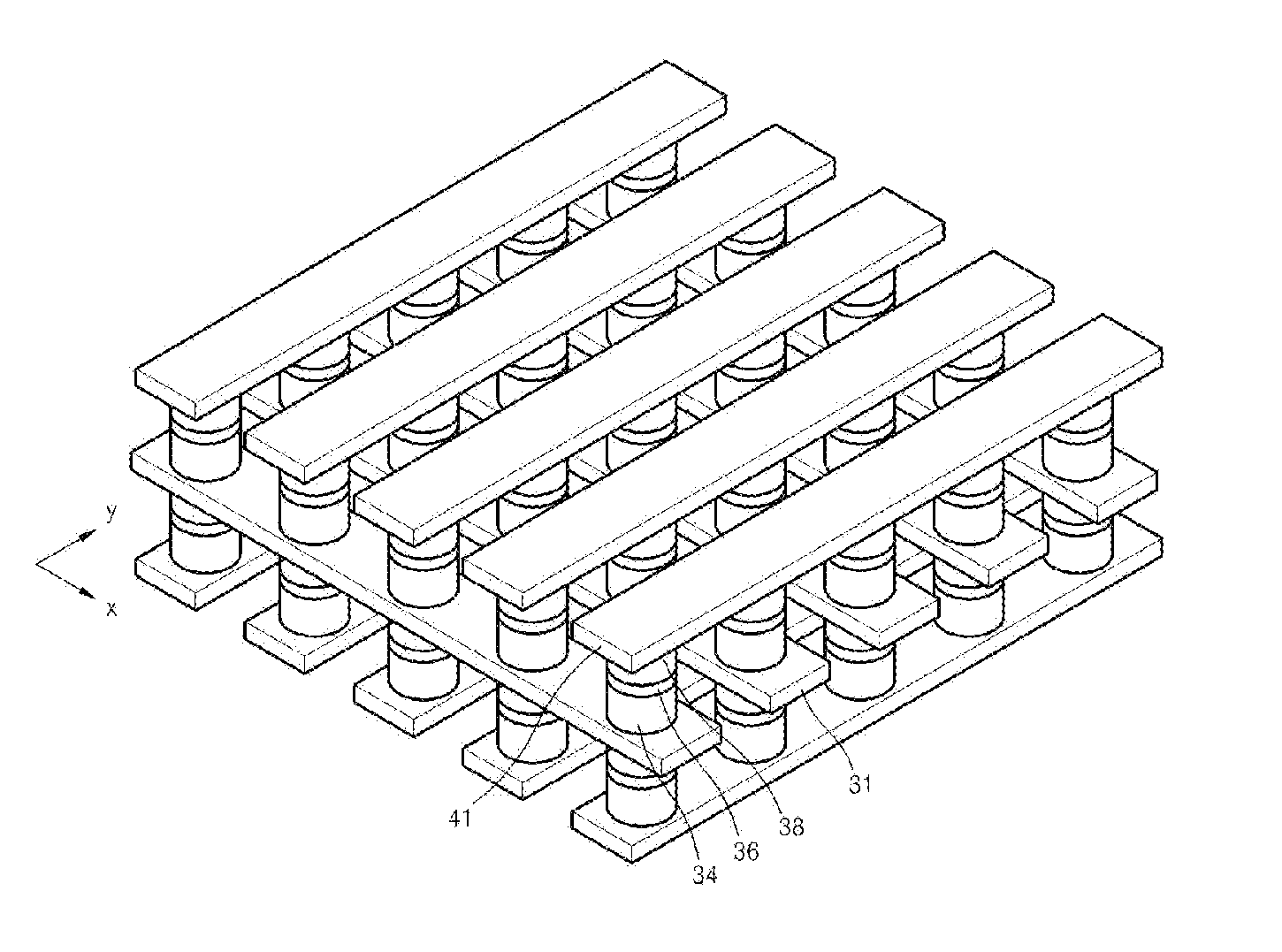
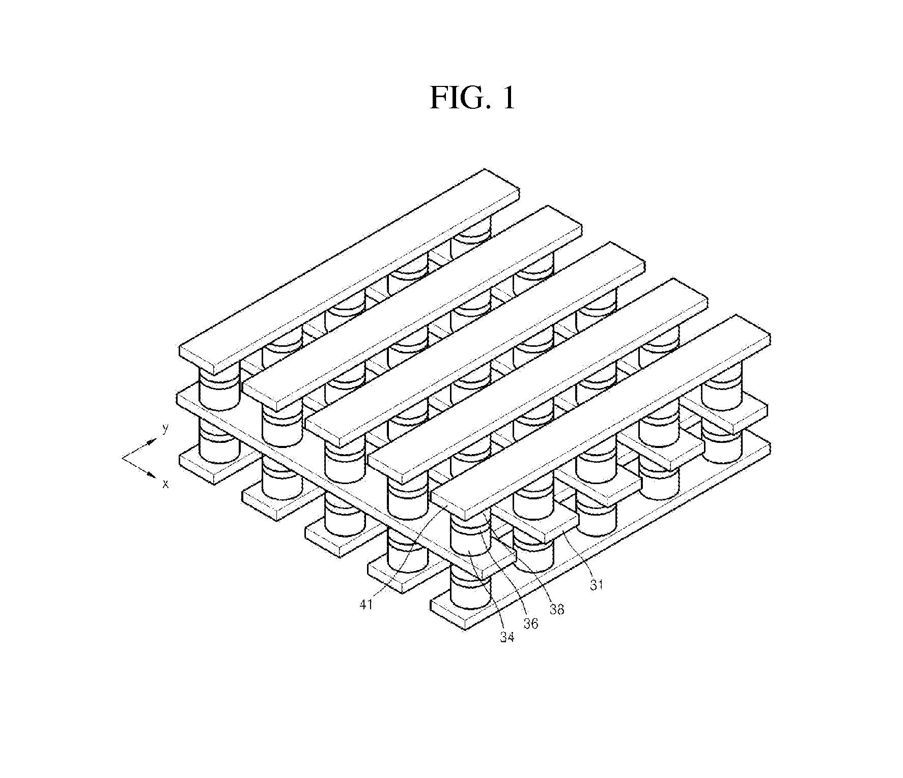
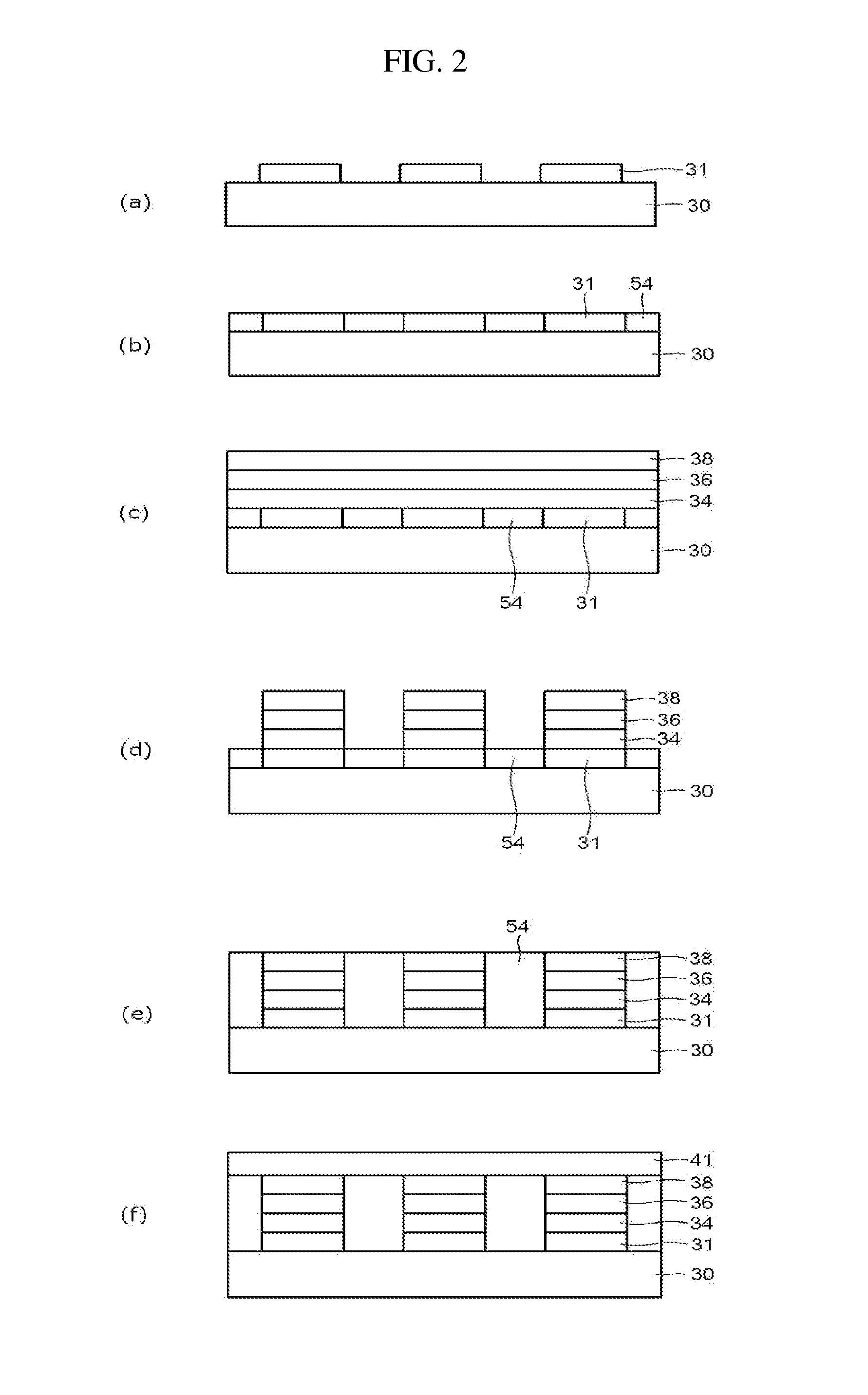
[0077]In one example, a silicon-containing chalconitride switching element was manufactured by forming a TiN upper electrode wiring on the silicon-containing chalconitride layer after forming a silicon-containing chalconitride layer on a TiN lower electrode wiring using photolithography method. The TiN lower electrode wiring and the TiN upper electrode wiring were arranged in such a direction that the TiN lower electrode wiring and the TiN upper electrode wiring crossed at a right angle. The TiN lower electrode wiring and the TiN upper electrode wiring had a line width of about 500 nm. A silicon-containing chalconitride layer having a size of about 500 nm×500 nm was formed between the TiN lower electrode wiring and the TiN upper electrode wiring at the intersecting point of the TiN lower electrode wiring and the TiN upper electrode wiring. A photograph from a scanning electron m...

example 2

Manufacturing of a Silicon-Containing Chalconitride Switching Element by N2 Plasma Treatment

[0081]In this example, a silicon-containing chalconitride switching element was manufactured by forming a TiN upper electrode wiring on the silicon-containing chalconitride layer having the nitride thin film after forming a silicon-containing chalconitride layer having a nitride thin film on a TiN lower electrode wiring using photolithography method. The TiN lower electrode wiring and the TiN upper electrode wiring were arranged in such a direction that the TiN lower electrode wiring and the TiN upper electrode wiring crossed at a right angle. The TiN lower electrode wiring and the TiN upper electrode wiring had a line width of about 500 nm. A silicon-containing chalconitride layer having a size of about 500 nm×500 nm was formed between the TiN lower electrode wiring and the TiN upper electrode wiring at the intersecting point of the TiN lower electrode wiring and the TiN upper electrode wiri...

example 3

Formation of a Silicon-Containing Chalconitride Layer

[0085]In this example, a silicon-containing chalconitride layer was formed on a substrate, and the silicon-containing chalconitride layer was treated by nitrogen plasma. Example x-ray photoelectron spectroscopy (XPS) analysis results for the silicon-containing chalconitride layer are shown in FIG. 8.

[0086]More specifically, FIG. 8A shows example analysis results for the silicon-containing chalconitride layer before performing nitrogen plasma treatment, FIG. 8B shows example analysis results obtained by high temperature deteriorating the silicon-containing chalconitride layer before performing nitrogen plasma treatment at about 450° C., and FIG. 8C shows example analysis results obtained by high temperature deteriorating the silicon-containing chalconitride layer after performing nitrogen plasma treatment at about 450° C.

[0087]In case of chalcogenides, out-diffusion of tellurium (Te) is generated (e.g., severely generated) after de...


PUM


Abstract

A switching element includes: a first electrode; a second electrode; and a silicon-containing chalconitride layer between the first electrode and the second electrode. A switching device includes: a threshold switch material layer between a first electrode and a second electrode. The threshold switch material layer includes a cationic metal element, a chalcogen element, a silicon element and a nitrogen element. A memory device include: a plurality of first wirings arranged in parallel with each other; a plurality of second wirings crossing the first wirings, and arranged in parallel with each other; and a memory cell formed at each intersection of the plurality of first wirings and the plurality of second wirings. The memory cell includes a laminate having a silicon-containing chalconitride layer, an intermediate electrode, and a memory layer.

Description

CROSS-REFERENCE TO RELATED APPLICATIONS[0001]This application claims priority under 35 U.S.C. §119 to Korean Patent Application No. 10-2012-0068177, filed on Jun. 25, 2012, and Korean Patent Application No. 10-2012-0125035, filed on Nov. 6, 2012, in the Korean Intellectual Property Office, the disclosures of which are incorporated herein in their entirety by reference.BACKGROUND[0002]1. Field[0003]Example embodiments relate to switching elements and devices, memory devices, and methods of manufacturing the same.[0004]2. Description of the Related Art[0005]Although a conventional switching device using a chalcogen compound of related art has excellent electrical properties, the switching device has a relatively low operating temperature of 400° C. or less. For instance, it is known that As2S3 has an operating temperature of about 150° C., As2Se3 has an operating temperature of about 200° C., As2Te3 has an operating temperature of about 250° C., As—Te—Ge has an operating temperature o...

Claims


Application Information

Patent Timeline
IPC IPC(8): H01L45/00
CPCH01L45/145H10B63/24H10B63/84H10N70/20H10N70/881H10N70/826H10N70/8833H10N70/026H10N70/041H10N70/883
Inventor LEE, DONG-SOOLEE, MYOUNG-JAECHUNG, U-IN
Owner SAMSUNG ELECTRONICS CO LTD
Why Eureka
Try Eureka