
Reactive bonding of a flip chip package

a flip chip and active bonding technology, applied in the field of flip chip bonding, can solve the problems of induced reliability problems, thermal warpage of packaging substrates, potential non-wet or unequal c4 solder heights, etc., and achieve the effect of minimizing heat and warpage of substrates

Inactive Publication Date: 2013-12-05
GLOBALFOUNDRIES US INC
View PDF2 Cites 4 Cited by
  • Summary
  • Abstract
  • Description
  • Claims
  • Application Information

AI Technical Summary

Benefits of technology

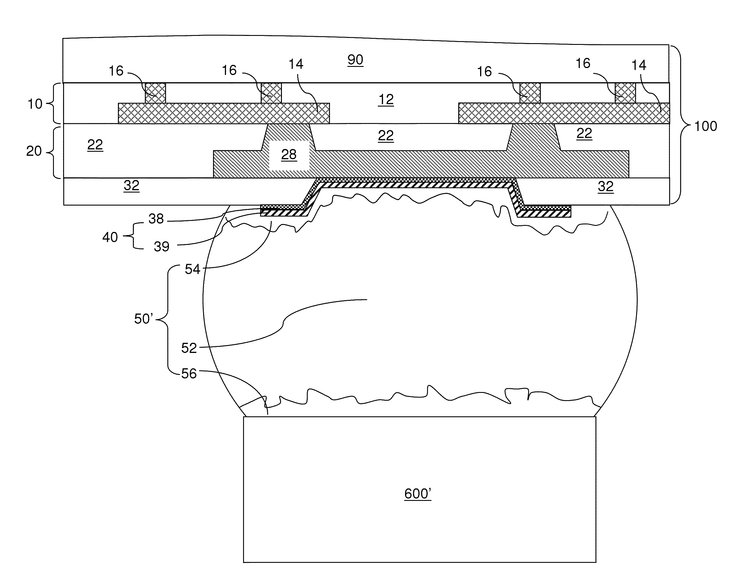
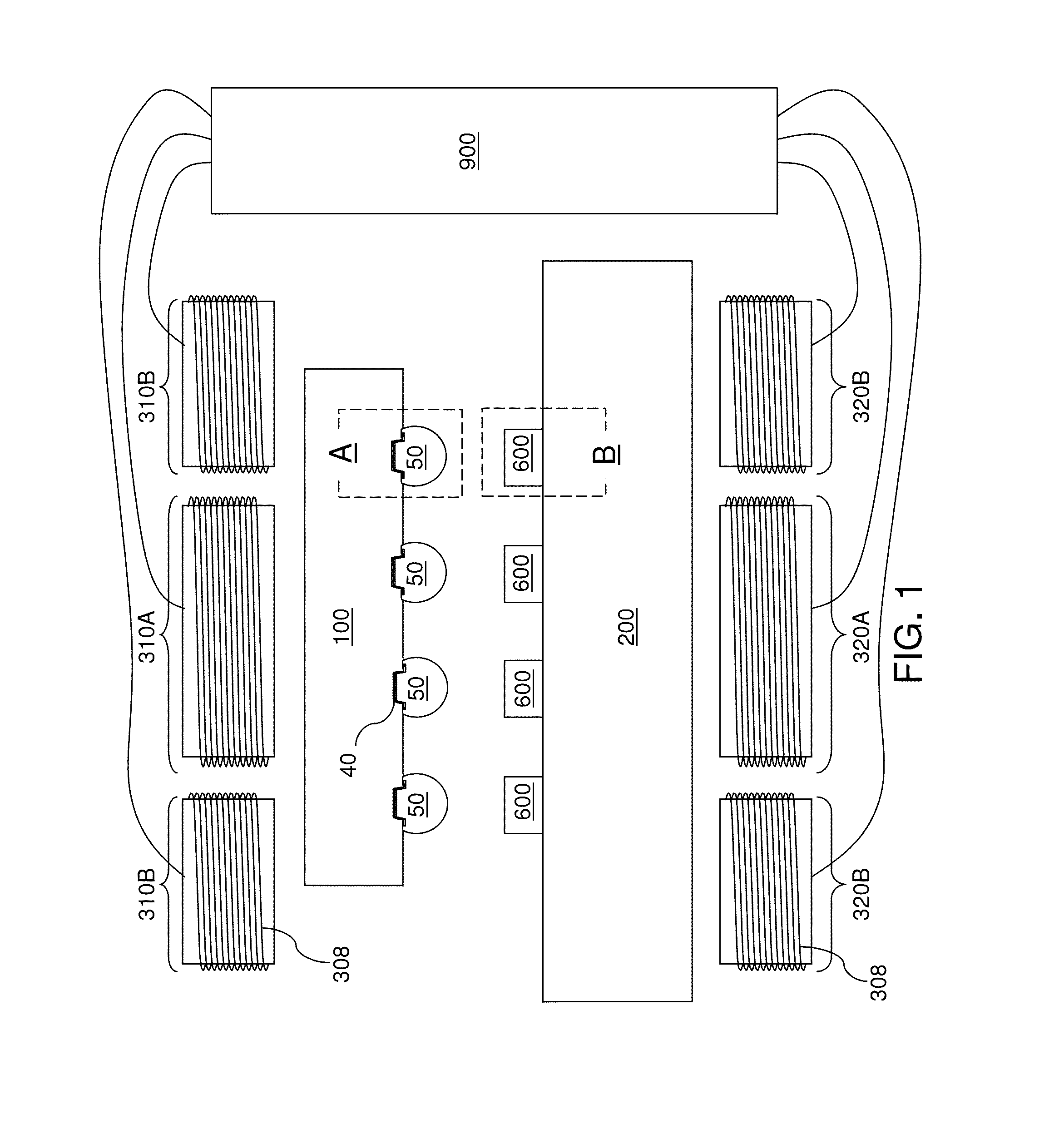
The patent describes a way to bond two materials together using magnetic heating. The process involves adding a set of reactive materials to a first substrate, which can be ignited by a magnetic field. The heat from the magnetic reaction melts solder balls on a second substrate, creating a strong bond. This method minimizes warping of the substrates during the bonding process.

Problems solved by technology

The thermal warp of the packaging substrate and the semiconductor chip causes alignment problems and stress-induced reliability problems for C4 bonding.
Particularly, the thermal warp of the packaging substrate poses a challenge because the thermal expansion coefficient of a packaging substrate tends to be greater than the thermal expansion coefficient of a semiconductor substrate.
Large thermal warp causes the packaging substrate to change shape during the heat up period prior to bonding, and leads to potential non-wets or unequal C4 solder heights.
Further, large thermal warp during the cool down period after the reflow of solder balls can lead to defects in the solder ball joints such as hot tears.

Method used


Image

  • Reactive bonding of a flip chip package
  • Reactive bonding of a flip chip package
  • Reactive bonding of a flip chip package

Examples


first embodiment

[0047]FIG. 3 illustrates a first example for a bonding pad 600, which includes a single stack or multiple stacks of a unit reactive-material-including stack 60. Referring to FIG. 4, a first example for the unit reactive-material-including stack 60 is illustrated according to the present disclosure.

[0048]In the first example of the unit reactive-material-including stack 60, two material layers are present. One of the two material layers includes the first material, and other of the two material layers includes the second material. A magnetic material can be selected for the first material and a non-magnetic material can be selected for the second material such that the first and second materials form a pair of reactive materials, which, upon ignition, react spontaneously to form an alloy or a composite of the first material and the second material.

[0049]The layer of the first material is herein referred to as a magnetic material layer 6, and the layer of the second material is herein...

second embodiment

[0052]Referring to FIG. 5, a second example for the unit reactive-material-including stack 60 is illustrated according to the present disclosure. In the second example of the unit reactive-material-including stack 60, three material layers are present. In this example, the first material and the second material are non-magnetic materials. The magnetic material is the additional material that is present in each of the unit reactive-material-including stack 60. One of the three material layers includes the first material, and is herein referred to as a first non-magnetic material layer 7. Another of the three material layers includes the second material, and is herein referred to as a second non-magnetic material layer 8′. Yet another of the three material layers includes the additional material, i.e., the magnetic material, and one of the first material and the second material. The layer that includes the additional material and one of the first and second materials is herein referre...

third embodiment

[0061]Referring to FIG. 6, a second example of a bonding pad 600 according to the present disclosure is illustrated. The second example of the bonding pad 600 includes a pair of a first material and a second material that constitute a set of reactive materials. The first material can be a magnetic material, and the second material can be a non-magnetic material.

[0062]The second example of the bonding pad 600 includes a matrix 6M of the first material and embedded non-magnetic particles 8P of the second material. An array of bonding pads 600 can be provided on the second substrate 200 by forming a material layer including a matrix of the first material embedding particles of the second material on the second substrate 200, and subsequently patterning the material layer to form the array of bonding pads 600. The matrix 6M of the first material and the embedded non-magnetic particles 8P of the second material can be formed by alternately depositing the first material and the second mat...


PUM

PropertyMeasurementUnit
thicknessaaaaaaaaaa
diameteraaaaaaaaaa
diameteraaaaaaaaaa

Abstract

An array of bonding pads including a set of reactive materials is provided on a first substrate. The set of reactive materials is selected to be capable of ignition by magnetic heating induced by time-dependent magnetic field. The magnetic heating can be eddy current heating, hysteresis heating, and / or heating by magnetic relaxation processes. An array of solder balls on a second substrate is brought to contact with the array of bonding pads. A reaction is initiated in the set of magnetic materials by an applied magnetic field. Rapid release of heat during a resulting reaction of the set of reactive materials to form a reacted material melts the solder balls and provides boding between the first substrate and the second substrate. Since the magnetic heating can be localized, the heating and warpage of the substrate can be minimized during the bonding process.

Description

BACKGROUND[0001]The present disclosure relates to semiconductor structures, and particularly to flip chip bonding employing bonding pads including reactive materials, and a structure for effecting the same.[0002]Once formation of semiconductor devices and interconnects on a semiconductor wafer (substrate) is completed, the semiconductor wafer is diced into semiconductor chips, or “dies.” Functional semiconductor chips are then packaged to facilitate mounting on a circuit board. A package is a supporting element for the semiconductor chip that provides mechanical protection and electrical connection to an upper level assembly system such as the circuit board. One typical packaging technology is Controlled Collapse Chip Connection (C4) packaging, which employs solder balls each of which contacts a C4 pad on the semiconductor chip and another C4 pad on a packaging substrate. Other packaging technologies employ micro C4's or C2's. The packaging substrate may then be assembled on the cir...

Claims


Application Information

Patent Timeline
Patent Type & Authority Applications(United States)
IPC IPC(8): H01L23/498H01L21/30
CPCH01L23/49811H01L2224/75264H01L2224/16501H01L24/13H01L24/16H01L24/75H01L24/81H01L2224/05582H01L2224/05624H01L2224/05639H01L2224/05644H01L2224/05647H01L2224/05655H01L2224/0566H01L2224/16238H01L2224/81192H01L2224/81222H01L2224/81455H01L2224/81457H01L2224/8146H01L2224/81815H01L2224/13006H01L2224/05572H01L2224/81466H01L2224/131H01L2924/00014H01L2224/0401H01L2224/16225H01L23/49866H01L2224/81121H01L2924/00012H01L2224/757H01L2924/014H01L2224/05552H01L24/17H01L25/0657H01L2224/13012H01L2224/13014H01L2224/13124H01L2224/13147H01L2224/13155H01L2224/13157H01L2224/1316H01L2224/13166H01L2224/13169H01L2224/13179H01L2224/16113H01L2224/16145H01L2224/16227H01L2224/1713H01L2224/17163H01L2224/7525H01L2224/818H01L2924/01014H01L2924/0541H01L2924/2064H01L2924/20641
Inventor FRITZ, GREGORY M.LEWANDOWSKI, ERIC P.
Owner GLOBALFOUNDRIES US INC
Learn More