Solderless Die Attach to a Direct Bonded Aluminum Substrate

a technology of aluminum substrate and die, which is applied in the direction of solventing apparatus, manufacturing tools, cooking vessels, etc., can solve the problems of dba-based power semiconductor devices that have been noticed to fail, aluminum is not readily solderable, and the ceramic or separation at the ceramic-to-copper interface is not easy to crack,

Active Publication Date: 2013-12-12
LITTELFUSE INC
View PDF3 Cites 62 Cited by
  • Summary
  • Abstract
  • Description
  • Claims
  • Application Information

AI Technical Summary

Benefits of technology

[0011]In a third example, there is no other layer of metal plating on the aluminum islands on the top side of the DBA panel assembly. Any native oxide on localized areas on top surfaces of the aluminum islands is mechanically removed. In one example, the thin layer of aluminum oxide on one such localized area is mechanically removed by using a micro-nozzle to blast a stream of small abrasive particles at the localized area. This blasting is done in an atmosphere substantially devoid of oxygen and devoid of moisture. The spent abrasive particles and any resulting debris are removed by an accompanying vacuum nozzle. The blasting mechanically removes aluminum oxide that may have grown on the localized area. After this mechanical cleaning step, silver nanoparticle paste is micro-jetted onto the cleaned aluminum surface using another micro-jet nozzle. Each localized area on an aluminum island that is to bear a sintered silver feature is cleaned and then deposited with silver nanoparticle paste in this way. The DBA panel assembly remains in an oxygen free environment between the cleaning step and the depositing of paste step, so aluminum oxide cannot regrow on the cleaned aluminum surface before the depositing step takes place. Sintering is then carried out on the entire panel assembly, thereby forming the desired sintered silver features. The DBA panel assembly is then cut to form individual DBA substrates. Accordingly, in the final DBA-based power device, there is no native aluminum oxide disposed between a sintered silver feature and the underlying aluminum island of the DBA substrate.

Problems solved by technology

In such applications, differential thermal expansion between the DBC ceramic and copper may result in cracking of the ceramic or in separation at the ceramic-to-copper interface.
Aluminum is not, however, a readily solderable metal.
In even more severe temperature cycling applications, DBA-based power semiconductor devices have been noticed to fail.

Method used


Image

  • Solderless Die Attach to a Direct Bonded Aluminum Substrate
  • Solderless Die Attach to a Direct Bonded Aluminum Substrate
  • Solderless Die Attach to a Direct Bonded Aluminum Substrate

Examples


Embodiment Construction

[0040]Reference will now be made in detail to some embodiments of the invention, examples of which are illustrated in the accompanying drawings. In the description and claims below, when a first object is referred to as being disposed “over” or “on” a second object, it is to be understood that the first object can be directly on the second object, or an intervening object may be present between the first and second objects. Similarly, terms such as “front”, “back”, “top” and “bottom” are used herein to describe relative orientations between different parts of the structure being described, and it is to be understood that the overall structure being described can actually be oriented in any way in three-dimensional space.

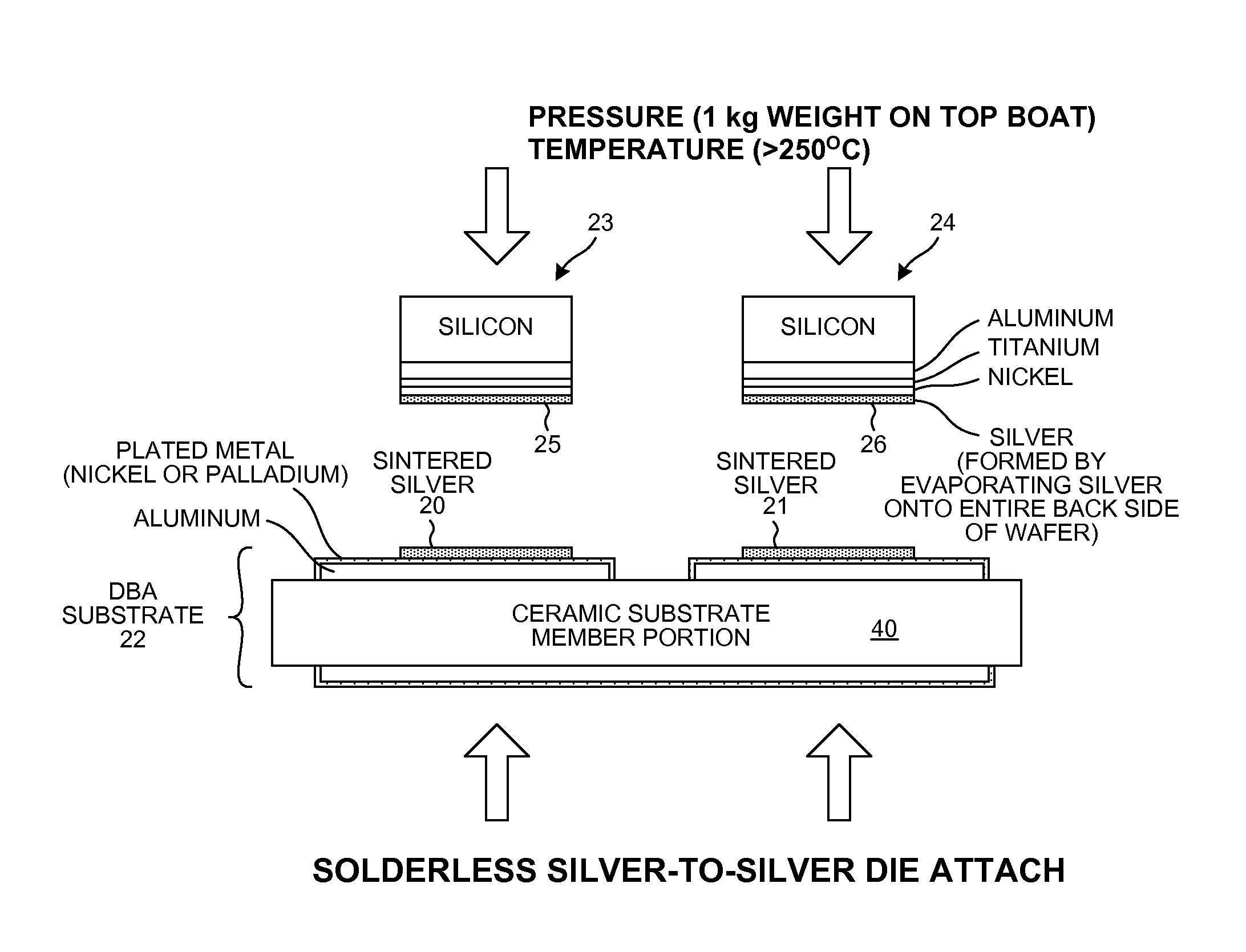
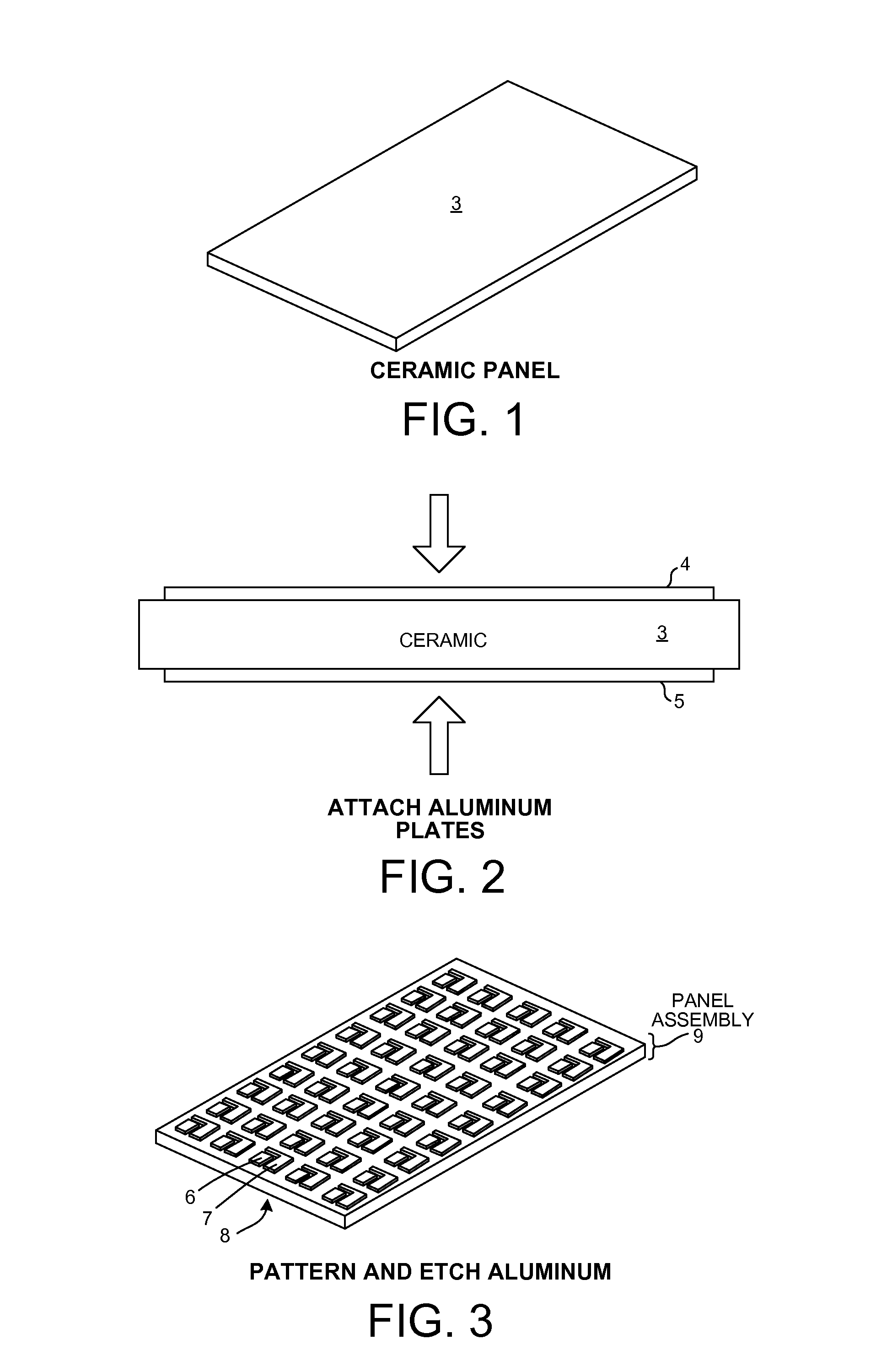
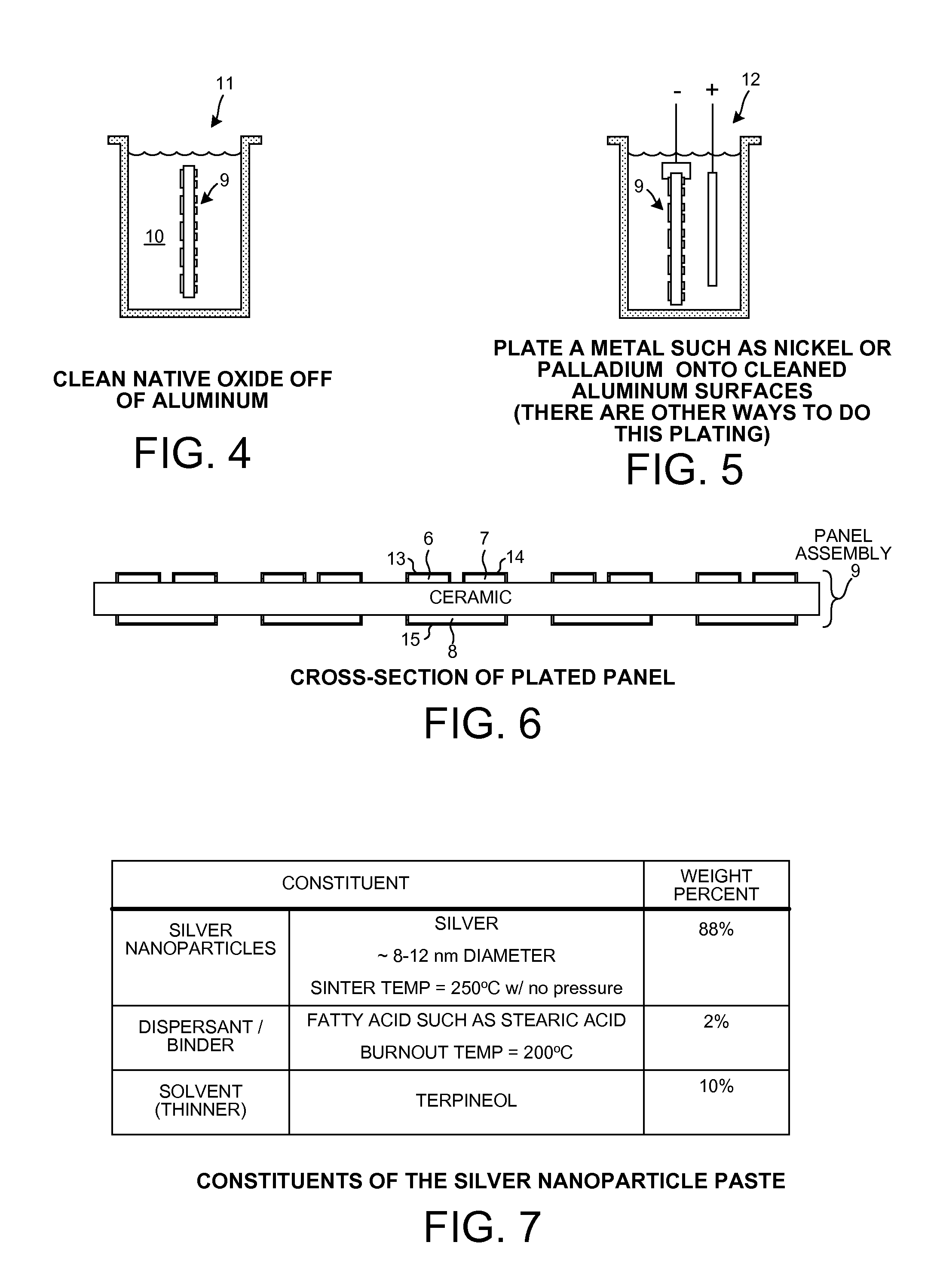
[0041]FIGS. 1-18 set forth a method of making a novel DBA-based power device 1 as illustrated in FIG. 17. The DBA-based power device 1 includes no soft solder disposed anywhere under the block of encapsulant 2 of the device. “Soft solders” melt at a temperature lower...


PUM

PropertyMeasurementUnit
weightaaaaaaaaaa
thickaaaaaaaaaa
temperatureaaaaaaaaaa

Abstract

A DBA-based power device includes a DBA (Direct Bonded Aluminum) substrate. An amount of silver nanoparticle paste of a desired shape and size is deposited (for example by micro-jet deposition) onto a metal plate of the DBA. The paste is then sintered, thereby forming a sintered silver feature that is in electrical contact with an aluminum plate of the DBA. The DBA is bonded (for example, is ultrasonically welded) to a lead of a leadframe. Silver is deposited onto the wafer back side and the wafer is singulated into dice. In a solderless silver-to-silver die attach process, the silvered back side of a die is pressed down onto the sintered silver feature on the top side of the DBA. At an appropriate temperature and pressure, the silver of the die fuses to the sintered silver of the DBA. After wirebonding, encapsulation and lead trimming, the DBA-based power device is completed.

Description

TECHNICAL FIELD[0001]The described embodiments relate to DBA-based power devices.BACKGROUND INFORMATION[0002]Direct-Bonded Copper (DBC) substrates (also called Direct Copper Bonded (DCB) substrates) are used extensively in the power semiconductor industry. A DBC substrate generally includes a thick ceramic substrate member, to which a thinner top plate of copper and a thinner bottom plate of copper are bonded. A semiconductor die includes one or more power devices such as, for example, power transistors and / or power diodes. Metallization on the back side of this semiconductor die is soldered to the top copper plate of the DBC. The DBC is often physically secured by soldering or welding the top copper plate to a package lead. Bond pads on the front side surface of the die are typically wirebonded to other package leads. The resulting assembly is then encapsulated. After lead trimming, ends of the leads protrude from the encapsulant. To improve conduction of heat from the package, the...

Claims


Application Information

Patent Timeline
Patent Type & Authority Applications(United States)
IPC IPC(8): H01L23/52B23K1/20B23K31/02
CPCH01L23/3735H01L23/488H01L23/49513H01L23/49562H01L23/49575H01L24/03H01L24/05H01L24/27H01L24/48H01L24/83H01L2224/27505H01L2224/83192H01L2224/80439H01L2224/2939H01L24/08H01L24/29H01L24/45H01L24/49H01L24/80H01L24/85H01L24/92H01L24/94H01L24/97H01L25/50H01L2224/031H01L2224/0332H01L2224/035H01L2224/03505H01L2224/0381H01L2224/04026H01L2224/05082H01L2224/05083H01L2224/05124H01L2224/05155H01L2224/05166H01L2224/05639H01L2224/05794H01L2224/05839H01L2224/08225H01L2224/27312H01L2224/2732H01L2224/275H01L2224/29139H01L2224/29339H01L2224/32227H01L2224/45124H01L2224/48229H01L2224/48247H01L2224/48472H01L2224/49111H01L2224/49112H01L2224/49171H01L2224/49176H01L2224/73265H01L2224/83203H01L2224/83455H01L2224/83464H01L2224/85181H01L2224/85424H01L2224/85455H01L2224/85464H01L2224/9222H01L2224/92247H01L2224/94H01L2224/97H01L2224/80203H01L2224/29294H01L2224/03312H01L2224/0589B23K20/2333H01L2924/351H01L2224/04042H01L2924/15787H01L2224/48724H01L2224/48755H01L2224/48764H01L2224/48739H01L2924/181H01L2224/48091B23K2101/34B23K2103/10B23K2103/56B23K2103/18H01L2924/00014H01L2224/80H01L2224/85H01L2224/03H01L2224/83H01L2224/05164H01L2924/00H01L2924/00012B23K1/20B23K31/02H01L23/52H01L25/0655H01L24/09
Inventor ZOMMER, NATHAN
Owner LITTELFUSE INC
Why Eureka
Try Eureka