Semiconductor integrated device assembly and related manufacturing process

a technology of integrated devices and manufacturing processes, which is applied in the direction of microstructural devices, electrostatic transducers of semiconductor, coatings, etc., can solve the problems of difficult manufacturing of the solution described above, limited freedom in designing the same acoustic chamber, and generally not optimized dimensions of the acoustic chamber of the transducer

Active Publication Date: 2013-12-19
STMICROELECTRONICS INT NV
View PDF6 Cites 22 Cited by
  • Summary
  • Abstract
  • Description
  • Claims
  • Application Information

AI Technical Summary

Benefits of technology

[0029]One embodiment of the present disclosure is to reduce the overall dimensions and optimization of the resulting electrical characteristics.

Problems solved by technology

The present Applicant has realized that the solution described above is somewhat complex to manufacture, due to the formation and stacked coupling of the two composite substrates.
In addition, the dimensions of the acoustic chambers of the transducer generally are not optimized, and the freedom in designing the same acoustic chambers may prove limited.

Method used


Image

  • Semiconductor integrated device assembly and related manufacturing process
  • Semiconductor integrated device assembly and related manufacturing process
  • Semiconductor integrated device assembly and related manufacturing process

Examples


Embodiment Construction

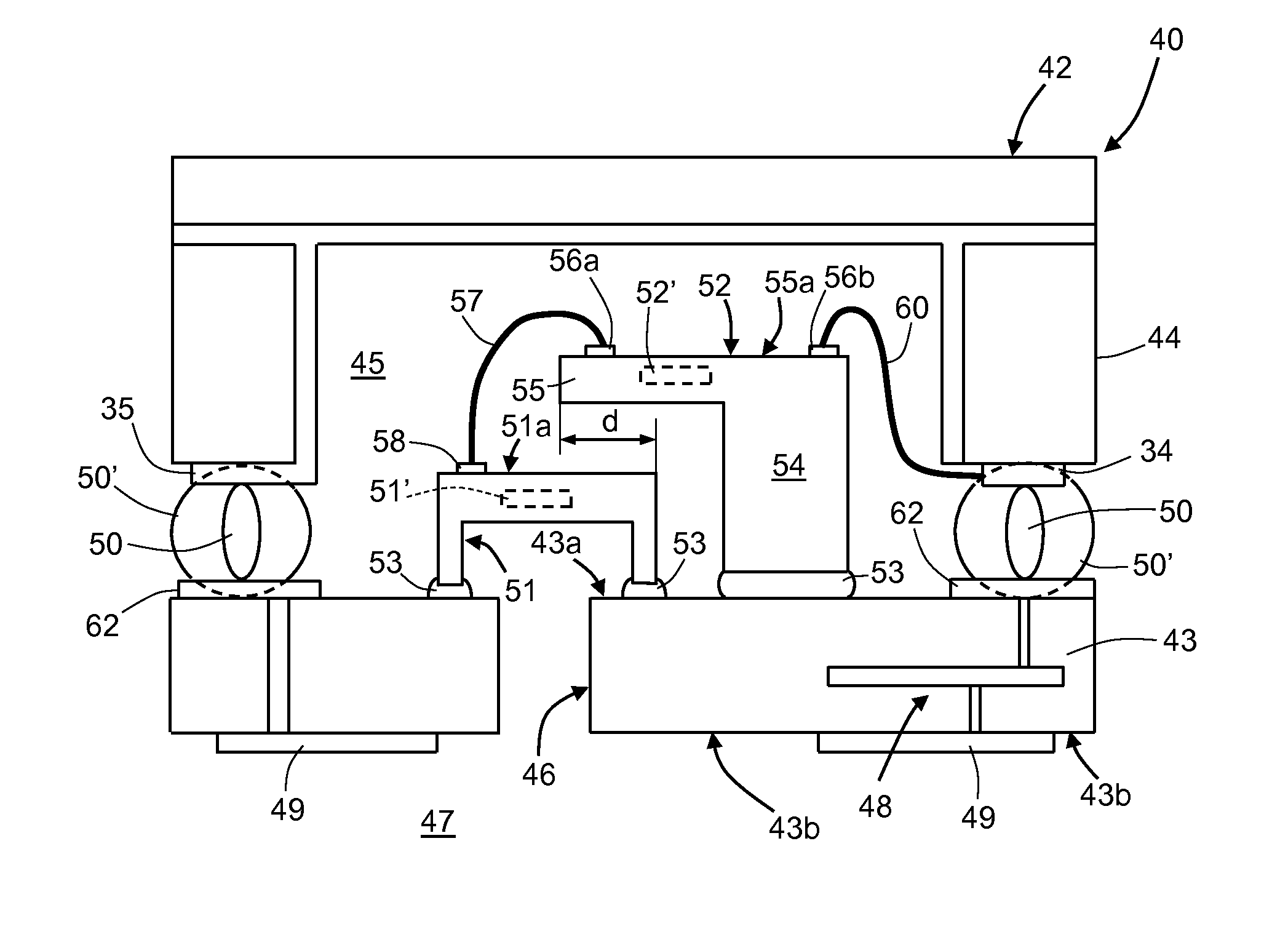
[0041]FIG. 4 shows an integrated semiconductor device, designated as a whole by 40, provided with a package 42, comprising a base substrate 43 and a cap element 44, with a substantially cup-shaped conformation, coupled to the base substrate 43 to define an empty internal space 45 within the package 42. Through the cap element 44, in particular throughout the thickness of a bottom wall thereof, an access opening 46 is provided, designed to set the internal space 45 in fluid communication with the external environment, designated as a whole by 47 (the access opening 46 constitutes the only outlet for the internal space 45).

[0042]In particular, the cap element 44 is a composite substrate, altogether equivalent to the composite substrates 21, 22 described with reference to FIG. 2, and hence obtained as described in FIGS. 3a-3c.

[0043]The base substrate 43 is, for example, constituted by a multilayer structure, made up of one or more layers of conductive material (generally metal) separa...


PUM

PropertyMeasurementUnit
distanceaaaaaaaaaa
vertical dimensionaaaaaaaaaa
conductiveaaaaaaaaaa

Abstract

Described herein is a semiconductor integrated device assembly, which envisages: a package defining an internal space; a first die including semiconductor material; and a second die, distinct from the first die, also including semiconductor material; the first die and the second die are coupled to an inner surface of the package facing the internal space. The second die is shaped so as to partially overlap the first die, above the inner surface, with a portion suspended in cantilever fashion above the first die, by an overlapping distance.

Description

BACKGROUND[0001]1. Technical Field[0002]The present disclosure relates to a semiconductor integrated device assembly and to a related manufacturing process. In particular, the following description will refer, without this implying any loss of generality, to the assembly of an acoustic transducer of a MEMS (microelectromechanical system) type.[0003]2. Description of the Related Art[0004]As acoustic transducer, for example a MEMS microphone of a capacitive type, generally comprises a micromechanical sensing structure, designed to transduce acoustic pressure waves into an electrical quantity (in the example a capacitive variation), and a reading electronics, designed to carry out appropriate processing operations (amongst which operations of amplification and filtering) of the electrical quantity to supply an electrical output signal, for example a voltage.[0005]In greater detail, and with reference to FIG. 1, a micromechanical sensing structure 1 of a MEMS acoustic transducer compris...

Claims


Application Information

Patent Timeline
Patent Type & Authority Applications(United States)
IPC IPC(8): B81B3/00B81C1/00
CPCB81B3/0021B81C1/00158H04R19/005H01L2224/48091H01L2224/48137H01L2924/16151H01L2924/16152H01L2924/00014
Inventor CONTI, SEBASTIANOVIGNA, BENEDETTO
Owner STMICROELECTRONICS INT NV
Why Eureka
Try Eureka