Method of manufacturing an LED

a manufacturing method and technology of led wafers, applied in the direction of solid-state devices, layered products, chemical instruments and processes, etc., can solve the problems of high environmental load, high yield, and easy cracking of led wafers, and achieve simple manufacturing and small environmental load. , the effect of high yield

Inactive Publication Date: 2014-01-02
NITTO DENKO CORP
View PDF0 Cites 11 Cited by
  • Summary
  • Abstract
  • Description
  • Claims
  • Application Information

AI Technical Summary

Benefits of technology

[0007]The present invention has been made to solve the above-mentioned conventional problem, and has an object to provide a method of manufacturing an LED with a small environmental load, which is simple and capable of manufacturing an LED with high yields by preventing damage to the LED wafer.
[0015]According to the present invention, in the back-grinding step, after the LED wafer is fixed to the table via the double-sided pressure-sensitive adhesive sheet, the LED wafer is ground. In this manner, the LED wafer may be prevented from being damaged to manufacture the LED with high yields. Further, according to the present invention, wax is unnecessary to fix the LED wafer, and hence application and cleaning of the wax are unnecessary. Therefore, the LED may be simply manufactured. Further, the use of cleaning liquid such as a solvent may be avoided, and hence the LED may be simply manufactured with a small environmental load. Further, an adverse effect to the LED due to the cleaning liquid may be prevented.

Problems solved by technology

Therefore, during the grinding, there is a problem in that damage such as cracking easily occurs in the LED wafer.
In addition, there are such problems that man-hours are required to apply and clean the wax, and that the environmental load is large because a solvent is used to clean the wax.
Moreover, there is a problem in that the LED is negatively affected by cleaning liquid.

Method used


Image

  • Method of manufacturing an LED
  • Method of manufacturing an LED
  • Method of manufacturing an LED

Examples


Embodiment Construction

A. Back-grinding Step

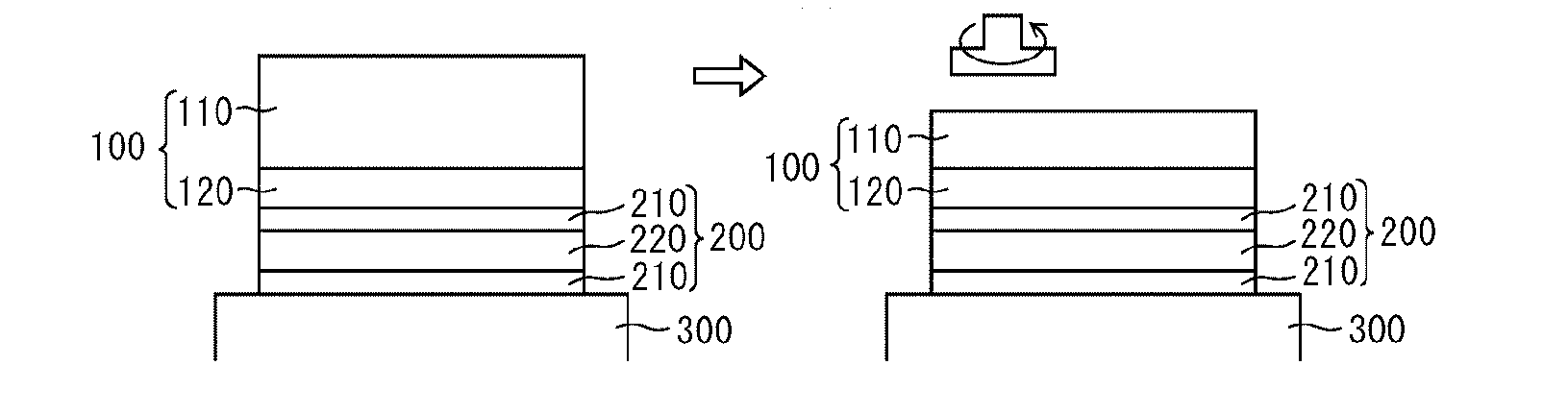
[0025]A method of manufacturing an LED of the present invention includes a back-grinding step of grinding a substrate of an LED wafer including a light emitting element and the substrate.

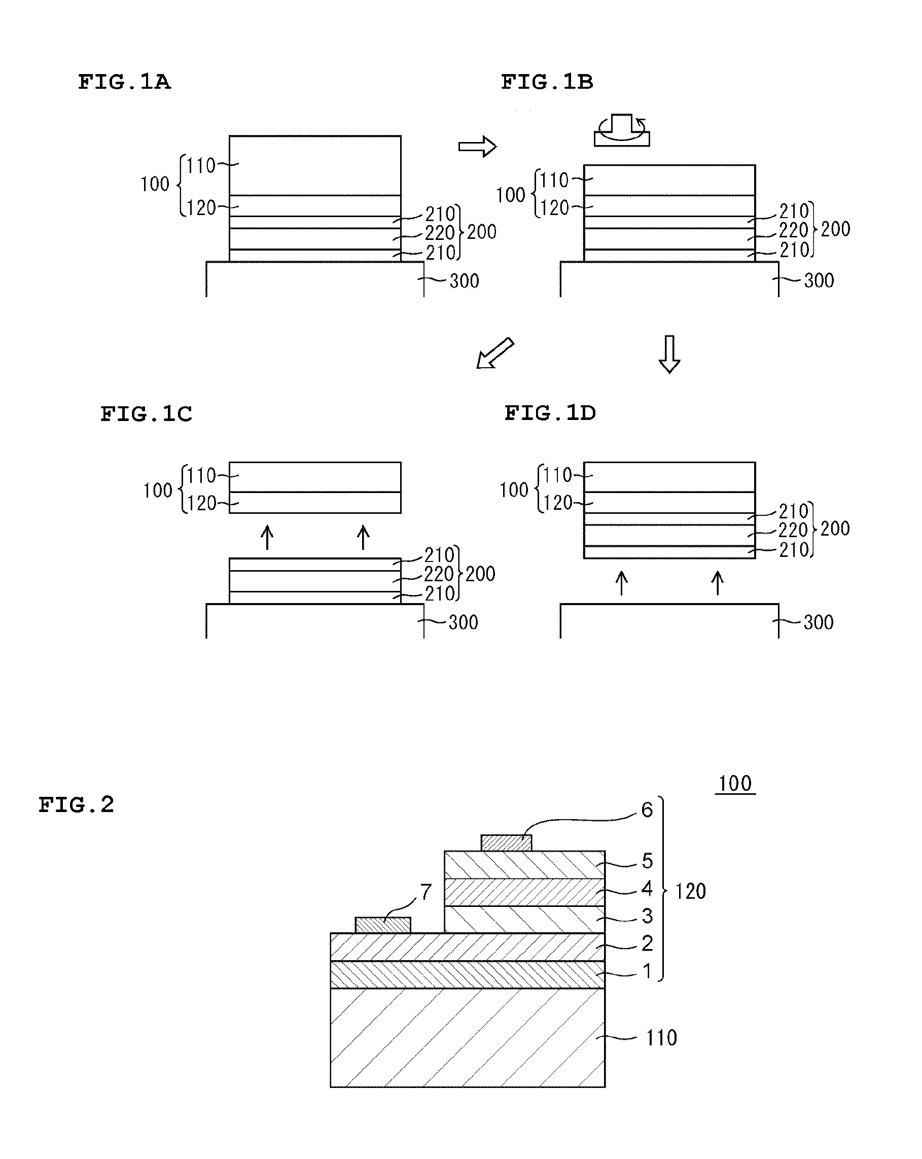
[0026]FIGS. 1A to 1D are schematic views illustrating a back-grinding step in a method of manufacturing an LED according to an embodiment of the present invention. Further, FIG. 2 is a schematic sectional view of an LED wafer 100. The LED wafer 100 includes a substrate 110 and a light emitting element 120. The substrate 110 is made of any appropriate material. Examples of the material for constituting the substrate 110 include sapphire, SiC, GaAs, GaN, and GaP. The effect of the present invention, that is, preventing damage to the LED wafer 100, is markedly obtained when the employed LED wafer 100 is made of such a hard and brittle material as those materials. The light emitting element 120 includes a buffer layer 1, an n-type semiconductor layer 2, a light emitting layer 3, a p...


PUM

PropertyMeasurementUnit
thicknessaaaaaaaaaa
thicknessaaaaaaaaaa
thicknessaaaaaaaaaa

Abstract

A method of manufacturing an LED according to an embodiment of the present invention includes back-grinding a substrate of an LED wafer including a light emitting element and the substrate, where the back-grinding includes fixing the LED wafer to a table via a double-sided pressure-sensitive adhesive sheet, and then grinding the substrate.

Description

[0001]This application claims priority under 35 U.S.C. Section 119 to Japanese Patent Application No. 2012-145449 filed on Jun. 28, 2012, which are herein incorporated by references.BACKGROUND OF THE INVENTION[0002]1. Field of the Invention[0003]The present invention relates to a method of manufacturing an LED.[0004]2. Description of the Related Art[0005]Hitherto, in manufacture of an LED, a light emitting element is laminated on a substrate to form an LED wafer, and then a surface of the substrate on a side opposite to the light emitting element is ground (back-ground) to thin the substrate (for example, Japanese Patent Application Laid-open Nos. 2005-150675 and 2002-319708). Generally, this grinding is carried out while fixing a surface of the substrate on the light emitting element side to a table via a pressure-sensitive adhesive wax. The LED wafer that has undergone grinding is subjected to, for example, steps of heating the wax to release the LED wafer, cleaning the wax adheri...

Claims


Application Information

Patent Timeline
Patent Type & Authority Applications(United States)
IPC IPC(8): H01L33/00
CPCH01L33/005H01L21/6836H01L24/27H01L33/0095H01L2221/68327H01L2221/6834H01L2221/68381H01L2224/83191H01L33/0093H01L2224/94H01L2924/12041H01L2924/12042H01L2924/00H01L2224/27H01L33/48
Inventor TAKAHASHI, TOMOKAZUAKIZUKI, SHINYASUGIMURA, TOSHIMASAMATSUMURA, TAKESHIUENDA, DAISUKE
Owner NITTO DENKO CORP
Why Eureka
Try Eureka