Field effect transistor

Active Publication Date: 2010-10-14
CANON KK
View PDF12 Cites 41 Cited by
  • Summary
  • Abstract
  • Description
  • Claims
  • Application Information

AI Technical Summary

Benefits of technology

[0024]An object of the present invention is to provide a field effect transistor using an amorphous oxide constituted by a small number of kinds of element

Problems solved by technology

However, it is difficult to produce an amorphous silicon TFT, a polysilicon TFT, and other TFT's on a substrate such as a plastic plate or foil since high-temperature processing is demanded for device production.
However, the organic semiconductor such as pentacene shows low thermal stability

Method used


Image

  • Field effect transistor
  • Field effect transistor
  • Field effect transistor

Examples


example 1

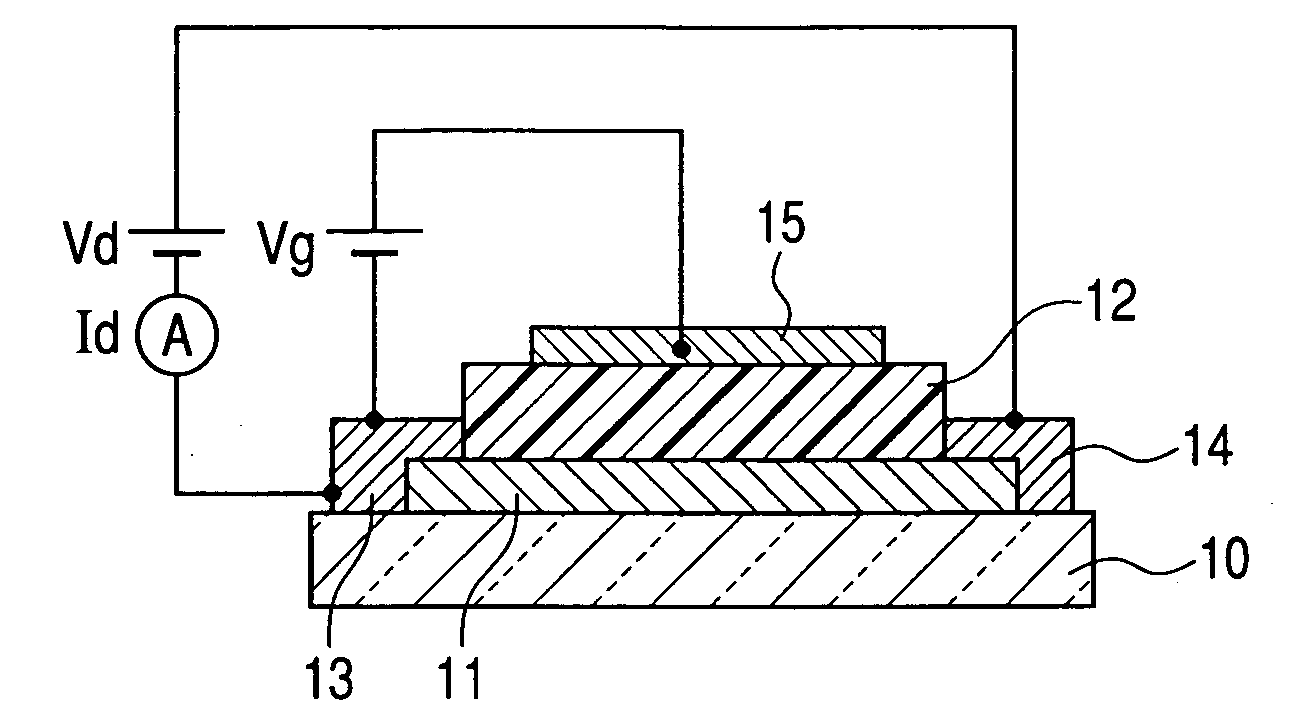
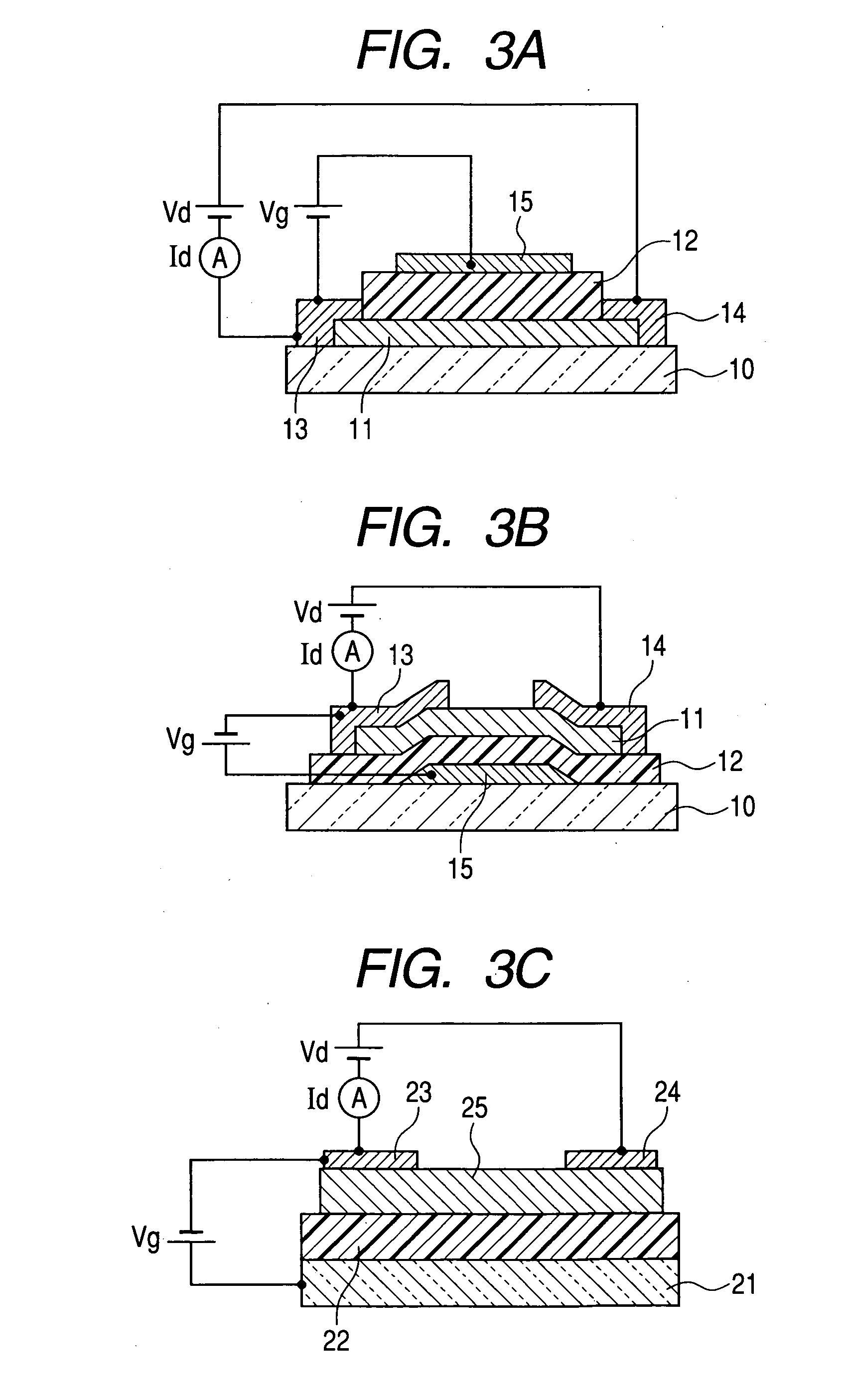
[0112]The present example is an example of producing a top gate type TFT illustrated in FIG. 3A in which a channel layer is an amorphous oxide of In—Si—O system.

[0113]At first, an amorphous oxide film of the In—Si—O system is formed as the channel layer on a glass substrate (product 1737 made by Corning Incorporated).

[0114]In the present example, the amorphous oxide film of the In—Si—O system is formed by radio-frequency sputtering method in the mixed atmosphere of argon gas and oxygen gas.

[0115]A sputtering film formation apparatus illustrated in FIG. 8 is used.

[0116]FIG. 8 includes a test sample 51, a target (material source) 52, a vacuum pump 53, a vacuum gauge 54, a substrate holding unit 55, gas flow controlling units 56 provided for respective gas introductory systems, a pressure controlling unit 57 and a film formation chamber 58.

[0117]The vacuum pump 53 serves as an exhaust unit for exhausting the gas from the interior of the film formation chamber 58. The substrate holding ...

example 2

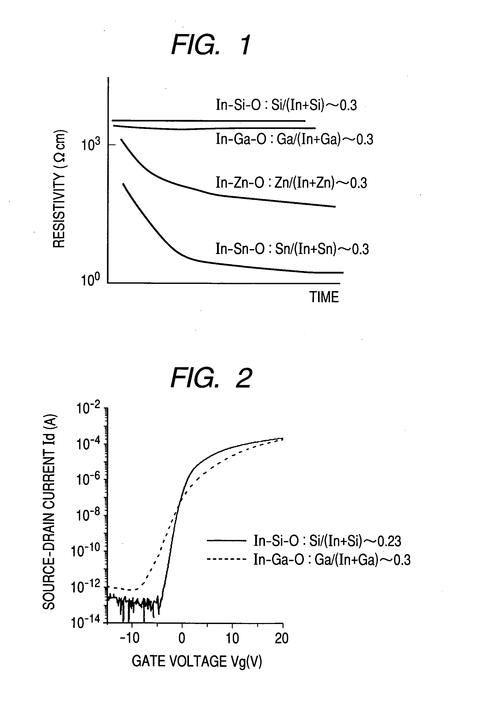
[0138]The present example is an example of experimental study on the composition dependency of In and Si in a thin film transistor with a channel layer containing In and Si as the principal components.

[0139]In the present example, in order to study the material composition dependency of the channel layer, combinatorial method is adopted for film formation. That is, experimental study is made with a technique of producing thin films of oxides having various compositions on one substrate at one time by the sputtering method. However, this technique does not necessarily have to be used to study it. The film formation may be carried out by preparing a material source (target) having a predetermined composition. By controlling the input power to each of a plurality of targets, a thin film with a desired composition may be formed.

[0140]In—Si—O films were formed by using sputtering apparatus with three cathodes. Since the targets are arranged in an oblique direction relative to the substra...

example 3

[0170]The present example is an example of applying an amorphous In—Zn—Si—O oxide semiconductor to the channel layer.

[0171]In addition, the present example is an example of producing a TFT having a configuration shown in FIG. 3B on a plastic substrate.

[0172]A polyethylene terephthalate (PET) film is used as the substrate. The channel length of the transistor is 60 μm. The channel width is 180 μm.

[0173]At first, a gate electrode 15 and a gate insulating layer 12 are patterned and formed on a PET substrate 10 by the photolithographic method and the liftoff technique.

[0174]The gate electrode 15 is made of a Ta film with a thickness of 50 nm. The gate insulating layer is a SiOxNy film with a thickness of 150 nm formed by the sputtering method. The relative permittivity of the SiOxNy film is approximately 6.

[0175]Next, the channel layer of the transistor was patterned and formed by the photolithographic method and the liftoff technique. The channel layer is made of an amorphous oxide 11a...


PUM

PropertyMeasurementUnit
Ratioaaaaaaaaaa

Abstract

A field effect transistor is provided including a gate electrode (15), a source electrode (13), a drain electrode (14) and a channel layer (11) to control current flowing between the source electrode (13) and the drain electrode (14) by applying a voltage to the gate electrode (15). The channel layer (11) is constituted of an amorphous oxide containing In and Si and having a compositional ratio expressed by Si/(In+Si) of not less than 0.05 and not more than 0.40.

Description

TECHNICAL FIELD[0001]The present invention relates to a field effect transistor and, in particular, relates to a field effect transistor utilized for a switching element of an LCD and an organic EL display.BACKGROUND ART[0002]A field effect transistor (FET) comprises a gate electrode, a source electrode and a drain electrode.[0003]The field effect transistor is an electronically active element wherein a voltage is applied to a gate electrode to control current flowing through a channel layer and control current between the source electrode and the drain electrode. In particular, an FET with a thin film, as a channel layer, which has undergone film formation on an insulating substrate made of ceramic, glass, plastic and the like, is called a thin film transistor (TFT).[0004]Thin film technology is applied to the above described TFT, which is, therefore, advantageously and easily formed on a substrate having a comparatively large area and is being widely used as a drive element of a f...

Claims


Application Information

Patent Timeline
IPC IPC(8): H01L29/786H01L29/26
CPCH01L29/7869H01L29/78606C23C14/086H01L21/324H01L29/78693
Inventor IWASAKI, TATSUYAITAGAKI, NAHO
Owner CANON KK
Why Eureka
Try Eureka