

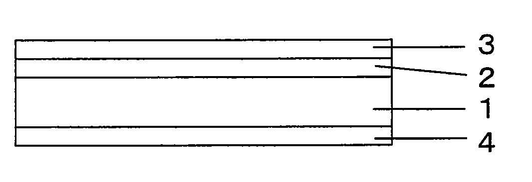
Conductive laminate and touch panel
a technology of conductive laminate and touch panel, which is applied in the direction of conductive layers on insulating supports, instruments, other domestic objects, etc., can solve the problems of yellowing of substrates, adverse influence of optical properties or electrical properties of electrode members, and damage to substrates, etc., to achieve the effect of satisfying the durability against hea
- Summary
- Abstract
- Description
- Claims
- Application Information
AI Technical Summary
Benefits of technology
Problems solved by technology
Method used
Image

Examples
example 1
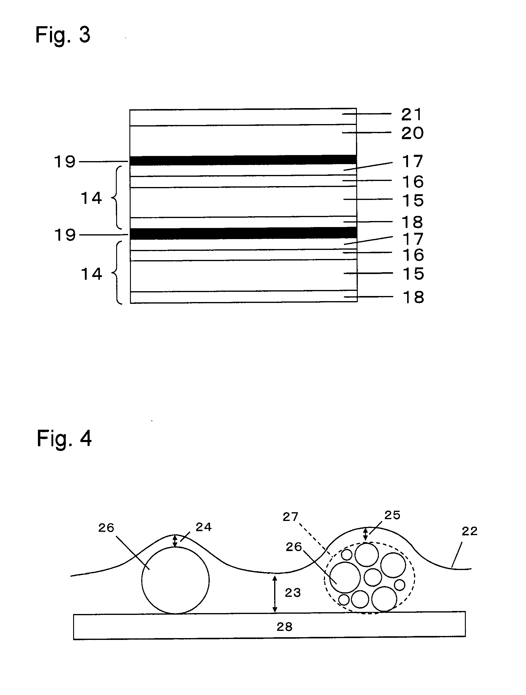
[0188]A 125 μm thick polyethylene terephthalate film, LUMIRROR (registered trademark) U48 (manufactured by Toray Industries, Inc.) was used as a substrate. Then, 100 g of the crosslinked layer material A and 1,026 g of benzene were mixed and stirred to prepare a crosslinked layer coating solution. The substrate was coated with the protective layer coating solution using a slit die coater mounted with shims made of SUS (thickness of shims 50 μm), and dried at 120° C. for 2 minutes to form a 950 nm thick crosslinked layer.
[0189]Then, the conductive layer A was formed on the surface opposite to the crosslinked layer of the substrate in the following manner.
[0190]Subsequently, 296 g of the protective layer material A and 704 g of ethyl acetate were mixed and stirred to prepare a protective layer coating solution. The above-mentioned conductive layer A was coated with the protective layer coating solution using a slit die coater mounted with shims made of SUS (thickness of shims 50 μm), ...
example 2
[0191]A 125 μm thick polyethylene terephthalate film, LUMIRROR (registered trademark) U48 (manufactured by Toray Industries, Inc.) was used as a substrate. Then, 500 g of the crosslinked layer material B and 1,382 g of ethyl acetate were mixed, followed by stirring to prepare a crosslinked layer coating solution. The substrate was coated with the protective layer coating solution using a slit die coater mounted with shims made of SUS (thickness of shims 50 μm), and dried at 120° C. for 2 minutes to form a 850 nm thick crosslinked layer.
[0192]Then, the conductive layer A was formed on the surface opposite to the crosslinked layer of the substrate in the following manner.
[0193]Subsequently, 500 g of the protective layer material A and 1,500 g of ethyl acetate were mixed, followed by stirring to prepare a protective layer coating solution. The above-mentioned conductive layer A was coated with the protective layer coating solution using a slit die coater mounted with shims made of SUS ...
example 3
[0194]A 125 μm thick polyethylene terephthalate film, LUMIRROR (registered trademark) U48 (manufactured by Toray Industries, Inc.) was used as a substrate. Then, 300 g of the crosslinked layer material C, 764 g of toluene and 764 g of methyl ethyl ketone were mixed and stirred to prepare a crosslinked layer coating solution. The substrate was coated with the protective layer coating solution using a slit die coater mounted with shims made of SUS (thickness of shims 50 μm), dried at 100° C. for 2 minutes and then irradiated with ultraviolet light at 1.2 J / cm2 for curing to form a 700 nm thick crosslinked layer.
[0195]Then, conductive layer B was formed on the surface opposite to the crosslinked layer of the substrate in the following manner.
[0196]Subsequently, 150 g of the protective layer material B, 3.60 g of the additive A, 7.15 g of the additive B and 1,907 g of ethyl acetate were mixed, followed by stirring to prepare a protective layer coating solution. The above-mentioned condu...
PUM
| Property | Measurement | Unit |
|---|---|---|
| thickness | aaaaa | aaaaa |
| thickness | aaaaa | aaaaa |
| dynamic friction coefficient | aaaaa | aaaaa |
Abstract
Description
Claims
Application Information