

Measuring/inspecting apparatus and measuring/inspecting method
a technology of measuring/inspecting apparatus and measuring/inspecting method, which is applied in the direction of material analysis using wave/particle radiation, instruments, nuclear engineering, etc., can solve the problems of lowering precision and inability to precisely measure/inspect, and achieve high precision of measuring/inspecting and shortening the settling time
- Summary
- Abstract
- Description
- Claims
- Application Information
AI Technical Summary
Benefits of technology
Problems solved by technology
Method used
Image

Examples
first embodiment
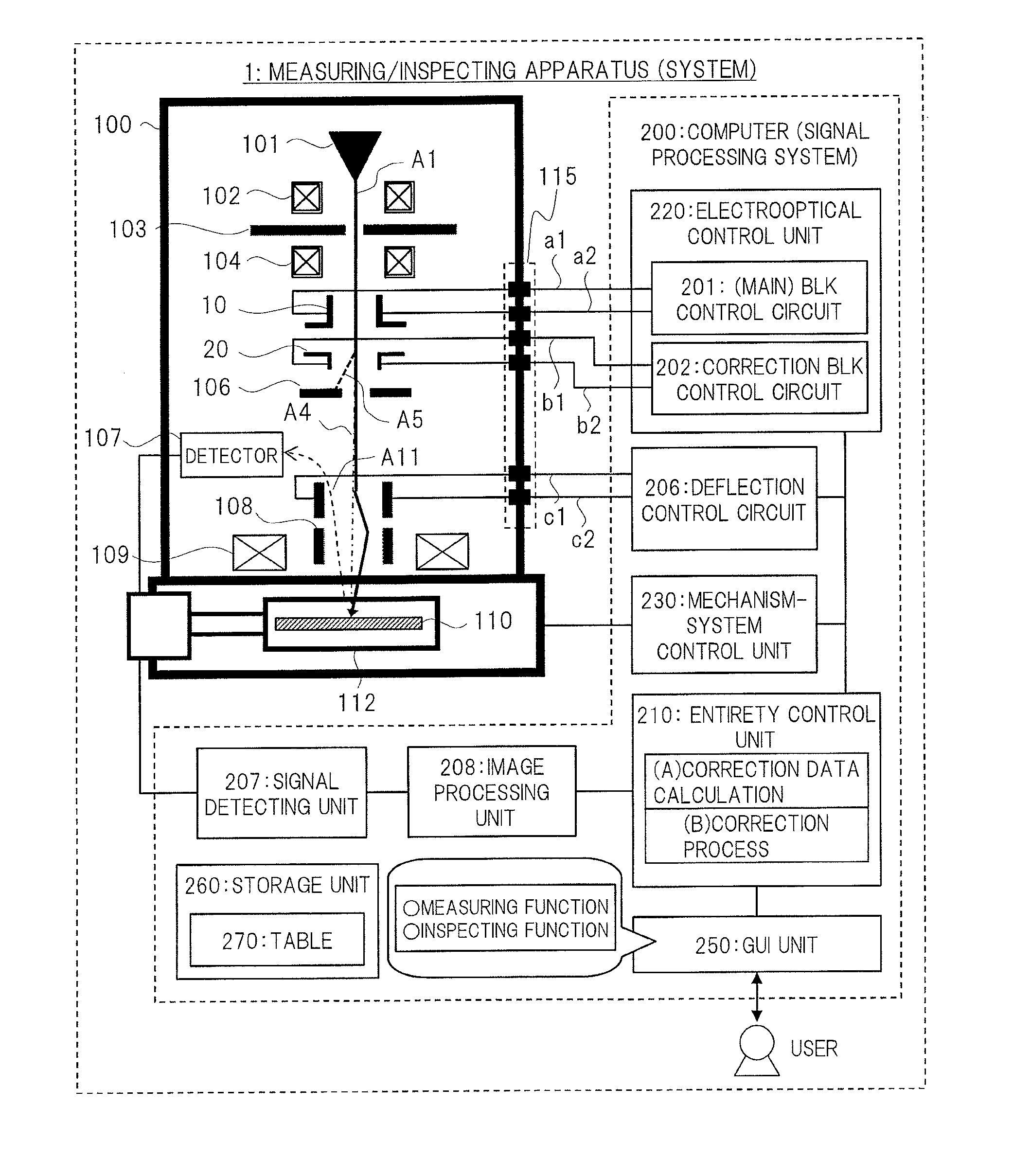
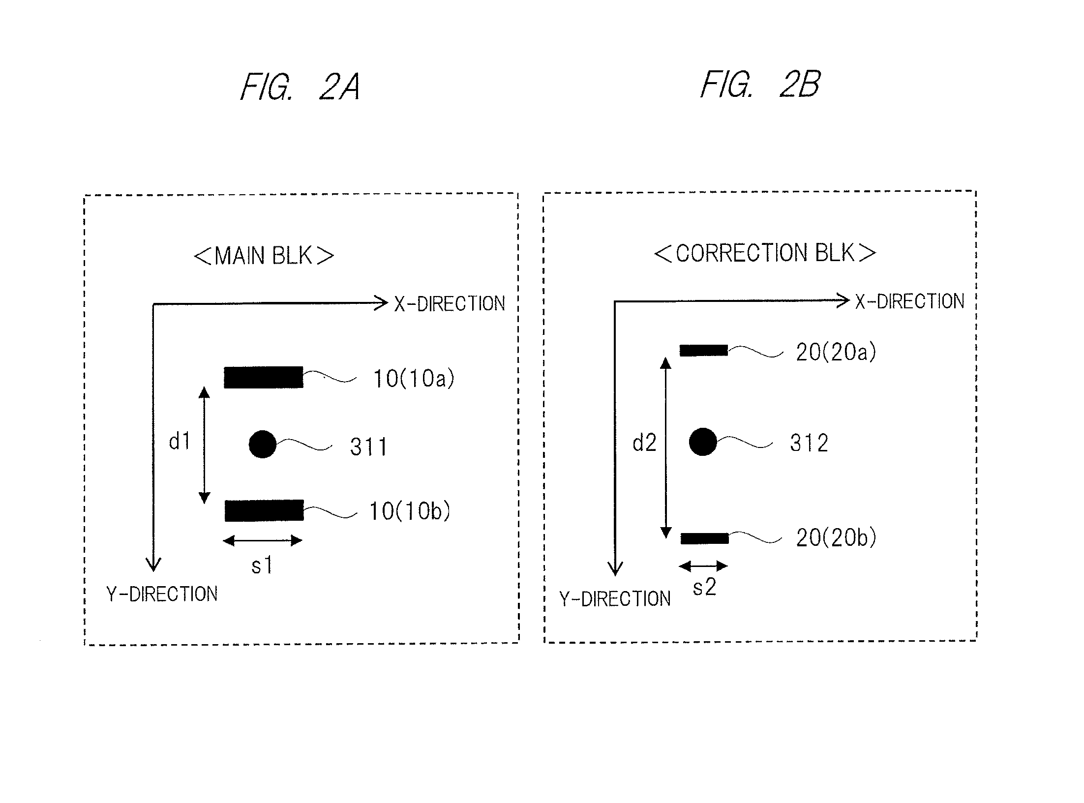
[0093]Based on the above-described conditions, a semiconductor measuring / inspecting apparatus of a scanning electron beam system of a first embodiment of the present invention and a measuring / inspecting method using the measuring / inspecting apparatus will be described with reference to FIGS. 1 to 9, etc. The first embodiment (FIG. 1, etc.) has a configuration in which, as BLK control electrodes which are elements for carrying out high-speed BLK control (high-speed ON / OFF switching control of irradiation / shutoff) along high-speed scanning of an electron beam, a correction BLK unit (the correction BLK control electrodes 20, the correction BLK control circuit 202, etc.) are newly added to the known main BLK unit (the main BLK control electrodes 10, the main BLK control 201, etc.) (FIG. 11). As a scanning system, the above-described raster scanning system, the vector scanning system, etc. can be used. As illustrated in FIGS. 2A and 2B, an electrode configuration is made such that each o...
second embodiment
[0155]Next, a semiconductor measuring / inspecting apparatus of the scanning electron beam system of a second embodiment of the present invention will be explained by using FIGS. 10A and 10B. Basic configurations of the apparatus of the second embodiment are similar to those of the first embodiment (FIG. 1, etc.), and different parts will be described below. In the second embodiment, as illustrated in FIG. 10, as the configuration of the BLK electrodes, the main BLK control electrodes 10 are comprised of four metal plates, and the correction BLK control electrodes 20 are also comprised of four metal plates. More specifically, BLK control in an arbitrary direction is configured to be enabled by independently controlling them in X-direction and Y-direction. In the second embodiment, the BLK control in the arbitrary direction can be carried out; therefore, scanning of an arbitrary pattern shape can be also flexibly supported limitations on applicable shapes / directions, etc. are reduced. ...
modification example
[0162]As another embodiment (modification example), not limited to the configuration of four BLK electrodes like the above-described second embodiment, a configuration of a plurality of electrodes (metal plates) and a control circuit in which consideration is made so that the beam deflection direction can be controlled to a desired direction may be employed. For example, not only a layout like a square shape consisting of four plates, but also a circular layout of six or more plate may be employed.
[0163]Moreover, as a modification example, the electrode configurations (the number, directions) of the main BLK and the correction BLK are not limited to be uniform like the first and second embodiments; and, for example, a configuration of a combination of two plates of the main BLK control electrodes 10 (FIG. 2A) and four plates of the correction BLK control electrodes 20 (FIG. 10B) may be employed. Thus, in that case, fine adjustment can be carried out by the correction BLK with respec...
PUM
 Abstract
Description
Claims
Application Information