Charge pump circuit with a brief settling time and high output voltage regulation precision

a pump circuit and settling time technology, applied in the direction of power conversion systems, instruments, dc-dc conversion, etc., can solve the problems of increasing the complexity of the circuit, the size of the integrated circuit transistor, and the supply voltage is reduced, so as to reduce the settling time and reduce the difference. , the effect of great speed and precision

Active Publication Date: 2007-02-13
MICRON TECH INC
View PDF12 Cites 24 Cited by
  • Summary
  • Abstract
  • Description
  • Claims
  • Application Information

AI Technical Summary

Benefits of technology

[0010]Another object is to provide a voltage booster circuit of the charge pump type in which the output voltage can be regulated with great speed and precision.
[0011]These and other objects are attained by a circuit for converting a direct current input voltage into an output voltage greater than the input voltage. The circuit includes a charge pump and a block for generating pulse signals of a predetermined frequency to be applied to a control input of the charge pump. The settling time, i.e. the time necessary for the output voltage to attain its operating value and to maintain it with a given precision, is reduced by providing the circuit with charge injection control via modulation of the duty cycle of the pulse signals as a function of the difference between the output voltage, or a predetermined fraction thereof, and a predetermined reference voltage and in such a manner as to reduce the settling time as the difference diminishes. The circuit includes a regulator that controls the charge pump based upon the predetermined reference voltage.

Problems solved by technology

These needs have led to a gradual reduction of the size of the transistors of the integrated circuits, a consequent reduction of the supply voltages and a growth of the complexity of the circuits.
The proper operation of non-volatile memories in general, and “flash” memories in particular, calls for relatively intense electric fields that cannot be obtained directly from the supply voltage of the device.
There may nevertheless occur the situation in which the charge pump has to work in a variable current regime, i.e. with absorption of current by the variable load in the course of time, so that the output voltage will not be as stable as would be desirable, but subject to a ripple.
The above discussion makes it clear that, given the numerous cell biasing operations that always call for non negligible settling times, the programming of a flash memory occupies a relatively long time.
In the case of a memory of the multilevel type, i.e. a memory in which the cells can be programmed at several threshold levels and are therefore capable of storing more than one bit per cell, this problem is particularly strongly felt, because the number of programming phases is greater and the sum of the settling times is therefore likewise greater.
Naturally, the problem related to the settling time concerns not only the programming of the cells, but also all the other operations in which the cell electrodes and the parasitic capacitances associated with them have to be biased with voltages generated by charge pumps.

Method used


Image

  • Charge pump circuit with a brief settling time and high output voltage regulation precision
  • Charge pump circuit with a brief settling time and high output voltage regulation precision
  • Charge pump circuit with a brief settling time and high output voltage regulation precision

Examples


Embodiment Construction

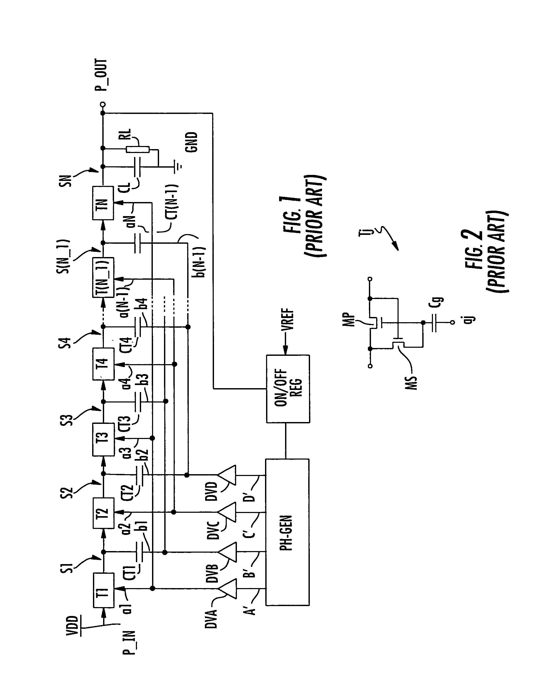
[0018]A charge pump converter typically utilized for generating some of the positive voltages necessary for the operation of a non-volatile memory is shown in FIG. 1. The charge pump circuit includes a multiplicity of stages S1–SN connected in cascade between an input terminal P-IN and an output terminal P-OUT. The input terminal is connected to a supply voltage source VDD and the output terminal is connected to a load represented by a capacitor CL and a resistance RL in parallel with each other. Each stage comprises a load transfer element T1–TN with an activation terminal a1–aN and, as charge storage element, a capacitor CT1–CT(N−1) connected between the output of the respective transfer element and a control terminal b1–b(N−1). An exception is in the last stage SN, the output of which is the output (P-OUT) of the converter and is connected to the load.

[0019]By way of example and as shown in FIG. 2, each of the charge transfer elements T1–TN may be formed by an N-channel MOS trans...


PUM


Abstract

A circuit for converting a direct current input voltage into an output voltage greater than the input voltage. The circuit includes a charge pump and a block for generating pulse signals of a predetermined frequency to be applied to a control input of the charge pump. The settling time, i.e. the time necessary for the output voltage to attain its operating value and to maintain it with a given precision, is reduced by providing the circuit with charge injection control via modulation of the duty cycle of the pulse signals as a function of the difference between the output voltage, or a predetermined fraction thereof, and a predetermined reference voltage and in such a manner as to reduce the settling time as the difference diminishes. The circuit includes a regulator that controls the charge pump based upon the predetermined reference voltage.

Description

FIELD OF THE INVENTION [0001]The present invention relates to a circuit for converting a direct current input voltage into a boosted output voltage, i.e. greater than the input voltage, with a charge pump and generation of pulse signals of predetermined frequency for controlling the charge pump circuit.BACKGROUND OF THE INVENTION [0002]Use of devices including non-volatile memories is becoming ever more widespread in a variety of electronic devices. In particular, the extensive use that is being made of mass consumer electronic equipment such as cellular telephones, portable audio reproducers and digital photographic and television cameras has led to a need for satisfying a growing demand for electronic devices having low power consumption and high memory capacity. These needs have led to a gradual reduction of the size of the transistors of the integrated circuits, a consequent reduction of the supply voltages and a growth of the complexity of the circuits. In fact, the need for as...

Claims


Application Information

Patent Timeline
Patent Type & Authority Patents(United States)
IPC IPC(8): G05F1/10H02M3/07
CPCH02M3/073
Inventor KHOURI, OSAMARAGONE, GIANCARLO
Owner MICRON TECH INC
Why Eureka
Try Eureka