Optical device using a plasmonic waveguide, and optical isolator

a technology of optical isolators and optical elements, which is applied in the direction of optical waveguide light guides, instruments, and high-speed optical amplifiers. it is difficult to grow magnetic garnets on substrates, and there is no report of any example in which other optical components are integrated on those semiconductors

Inactive Publication Date: 2014-01-09
NAT INST OF ADVANCED IND SCI & TECH
View PDF2 Cites 9 Cited by
  • Summary
  • Abstract
  • Description
  • Claims
  • Application Information

AI Technical Summary

Benefits of technology

[0023]Other and further features and advantages of the invention will appear more f...

Problems solved by technology

It is impossible to allow optical elements, such as high-speed optical amplifiers and high-speed laser diodes, to operate normally, without any optical isolators.
In further integration of the optical integrated circuits, reflected light that is reflected off from optical components and back-traveling causes unstable operation of a device in interest, resulting in a conspicuous problem.
However, such the optical isolators are one of the optical components that are not integrated into OICs.
It is difficult to grow the magnetic garnets on substrates, such as Si, GaAs, and InP, which are used as substrates for OICs; however, some methods are reported.
However, there is no report of any example in which other optical components are integrated on those semiconductor substrates having optical isolators integrated therein.
When the quality of magnetic garnets or diluted magnetic semiconductors is low, their magneto-optical constants become low to result in a high optical loss.
Even if the crystal quality of those magneto-optical materials is maintained during the step of integrating an optical isolator into an OIC, the crystal quality of those magneto-optical materials becomes worse upon the step of integrating other optical components thereinto.
This is the reason why any optical isolators, which are fabricated using magnetic garnets or diluted mag...

Method used


Image

  • Optical device using a plasmonic waveguide, and optical isolator
  • Optical device using a plasmonic waveguide, and optical isolator
  • Optical device using a plasmonic waveguide, and optical isolator

Examples


first embodiment

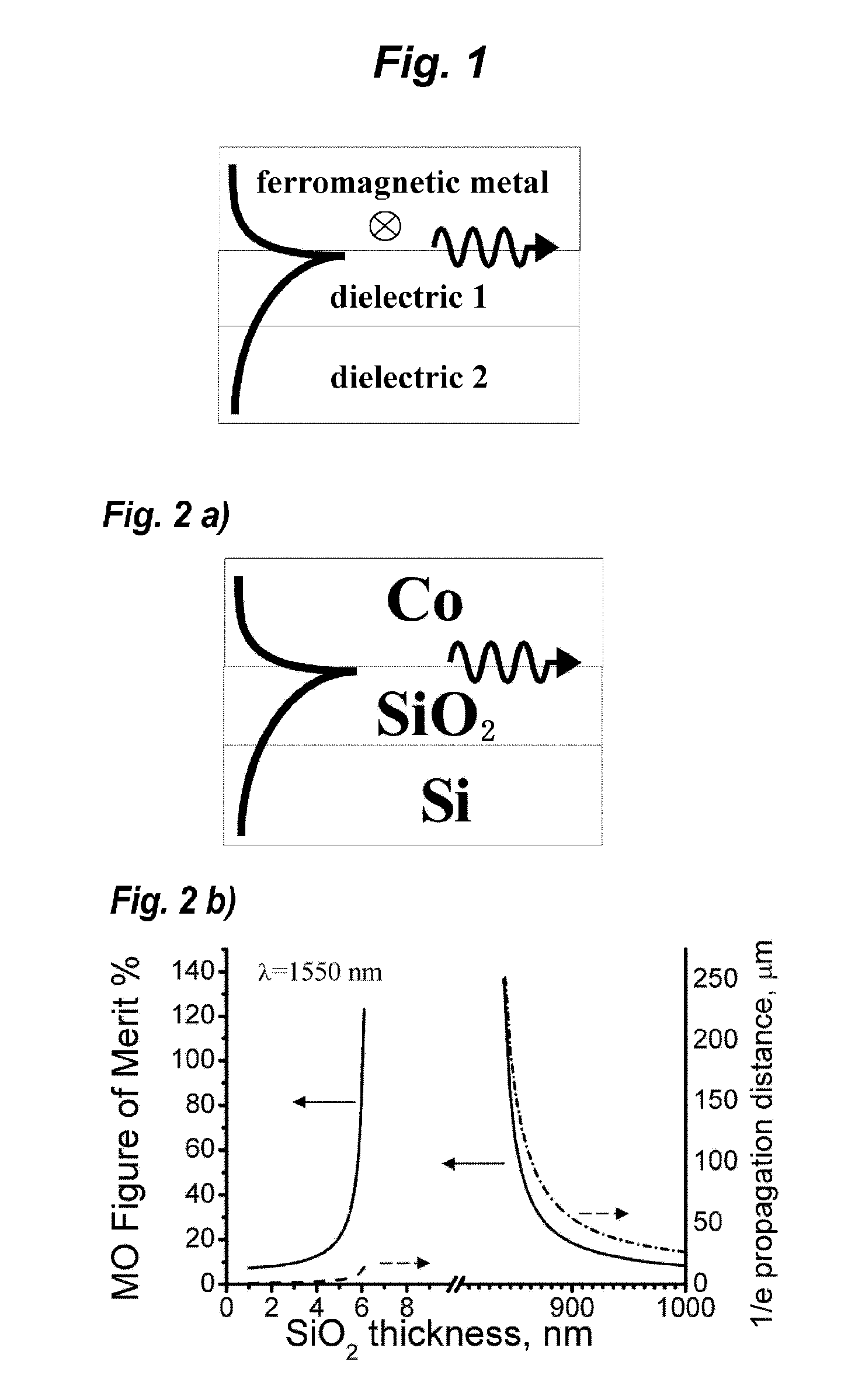
[0066]This embodiment relates to a plasmonic waveguide of three layers composed of Co / SiO2 / Si. This embodiment is described, with referring to FIGS. 2a) and 2b). FIG. 2a) is a diagram showing a structure of the plasmonic waveguide that was fabricated on a Si substrate. A SiO2 layer was interposed between the Si substrate and a Co layer. FIG. 2b) is a graph showing the results of a propagation distance where plasmons attenuated to 1 / e (right-side vertical axis) and a magneto-optical figure-of-merit (left-side vertical axis), each to the layer thickness of SiO2. In FIG. 2a), a magnetic field was applied to perpendicularly to a propagation direction of the plasmons. FIG. 2a) is a diagram showing the case where light entered from left on the drawing plane, and the direction of magnetization of the ferromagnetic metal layer Co was one perpendicularly entering the drawing plane in FIG. 2a) (i.e. a forward direction). This is an example of using light of wavelength 1,550 nm. In FIG. 2b), a...

second embodiment

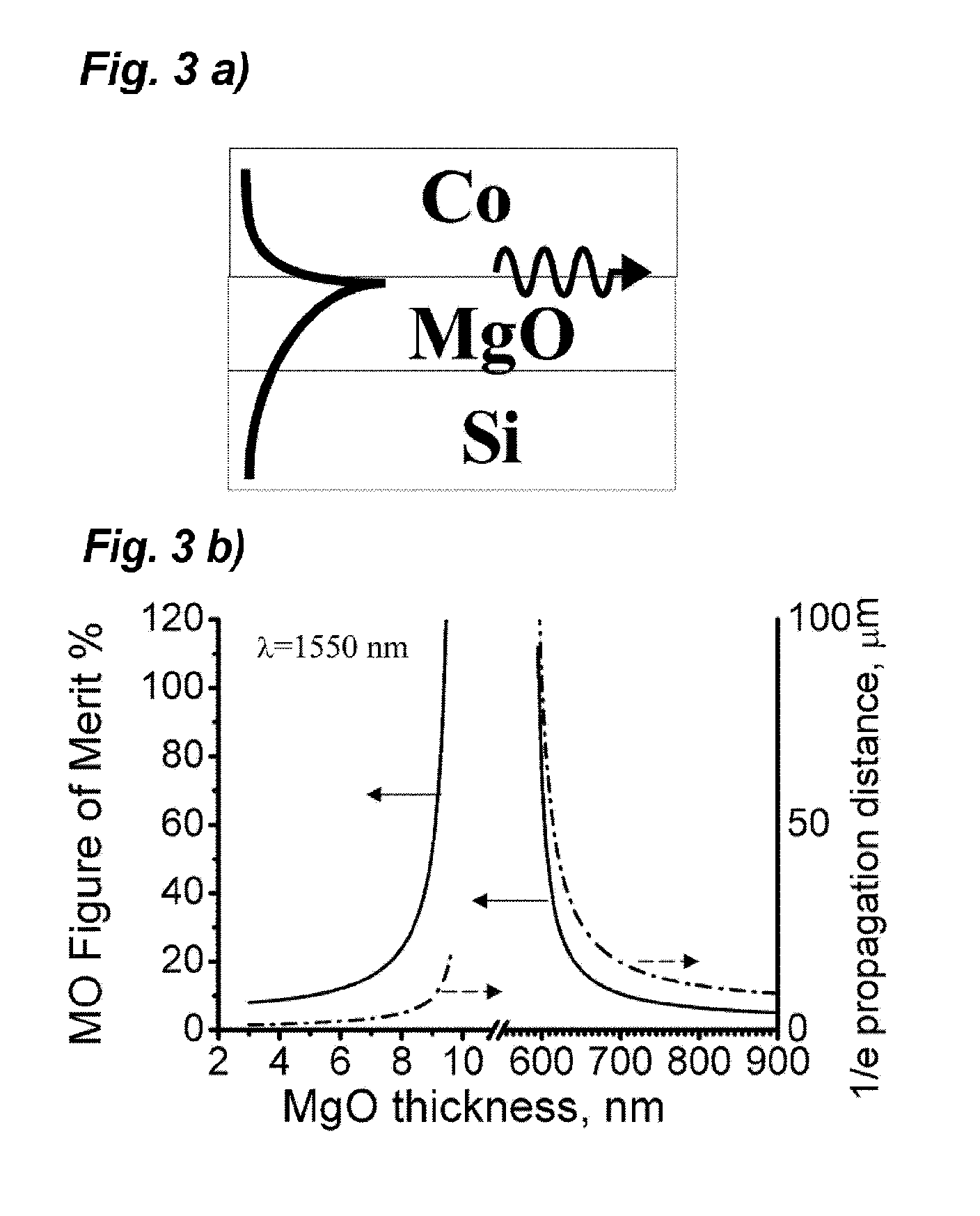
[0071]This embodiment relates to a plasmonic waveguide of three layers composed of Co / MgO / Si. This embodiment is described, with referring to FIGS. 3a) and 3b). FIG. 3a) is a diagram showing a structure of the plasmonic waveguide that was fabricated on a Si substrate. A MgO layer was interposed between the Si substrate and a Co layer. FIG. 3b) is a graph showing the results of a propagation distance where plasmons attenuated to lie (right-side vertical axis) and a magneto-optical figure-of-merit (left-side vertical axis), each to the layer thickness of MgO. Similar to the first embodiment, in FIG. 3a), a magnetic field was applied to perpendicularly to a propagation direction of the plasmons. This is an example of using light of wavelength 1,550 nm. When the layer thickness of MgO approached the range of from 9.6 nm to 595 nm, the magneto-optical figure-of-merit sharply enhanced. In this embodiment, the plasmonic waveguide has an excellent performance as an optical isolator, when th...

third embodiment

[0075]This embodiment relates to a plasmonic waveguide of three layers composed of Fe / SiO2 / Si. This embodiment is described, with referring to FIGS. 4a) and 4b). FIG. 4a) is a diagram showing a structure of the plasmonic waveguide that was fabricated on a Si substrate. A SiO2 layer was interposed between the Si substrate and a Fe layer. FIG. 4b) is a graph showing the results of a propagation distance where plasmons attenuated to 1 / e (right-side vertical axis) and a magneto-optical figure-of-merit (left-side vertical axis), each to the layer thickness of the SiO2 layer. Similar to the first embodiment, in FIG. 4a), a magnetic field was applied to perpendicularly to a propagation direction of the plasmons. This is an example of using light of wavelength 1,550 nm. When the layer thickness of the SiO2 layer approached the range of from 8.4 nm to 600 nm, the magneto-optical figure-of-merit sharply enhanced. In this embodiment, the plasmonic waveguide has an excellent performance as an o...


PUM


Abstract

An optical device having a plasmonic waveguide, in which the plasmonic waveguide has a layered structure of at least three layers that a ferromagnetic metal layer, a first dielectric layer, and a second dielectric layer are layered in this order, in which the first and second dielectric layers are layers that allow light to be transmitted therethrough, and in which a refractive index of the second dielectric layer is higher than a refractive index of the first dielectric layer; and an optical isolator, having the optical device.

Description

FIELD OF THE INVENTION[0001]The present invention relates to an optical device using a novel plasmonic waveguide, and an isolator which is a representative example of the optical device.BACKGROUND OF THE INVENTION[0002]In optical communication systems and other optical application systems, optical devices, such as optical isolators, are indispensable components. For example, an optical isolator is utilized to prevent reflected light, which is reflected and back-traveling, from entering or being incident to optical elements. It is impossible to allow optical elements, such as high-speed optical amplifiers and high-speed laser diodes, to operate normally, without any optical isolators.[0003]Integration of optical elements into optical integrated circuits (OICs) is necessary to lower production costs and to enhance the performance of high-speed optical data processing for high-speed optical networks. In further integration of the optical integrated circuits, reflected light that is ref...

Claims


Application Information

Patent Timeline
IPC IPC(8): G02B6/10
CPCG02B6/10G02B6/12004G02B6/1226B82Y20/00
Inventor ZAYETS, VADYMANDO, KOJISAITO, HIDEKAZUYUASA, SHINJI
Owner NAT INST OF ADVANCED IND SCI & TECH
Why Eureka
Try Eureka