Plasmon lasers at deep subwavelength scale

a laser and subwavelength technology, applied in the field of laser light sources, can solve the problems of limited lasers, both in optical mode size and physical device dimension, and achieve the effects of large modulation bandwidth, large modulation bandwidth, and efficient generation of sub-wavelength high intensity ligh

Active Publication Date: 2013-08-13
RGT UNIV OF CALIFORNIA
View PDF7 Cites 8 Cited by
  • Summary
  • Abstract
  • Description
  • Claims
  • Application Information

AI Technical Summary

Benefits of technology

[0013]An aspect of the present invention is a nanometer scale semiconductor laser source for on-chip integration. The laser can be very compact, with typical device dimensions of 50-200 nm×50-200 nm×2-20 μm. The device is capable of efficient generation of sub-wavelength high intensity light and the potential for large modulation bandwidth >1 THz.
[0014]The high efficiency and compact dimensions are achieved by the laser action of optical modes bound between the surface of a metal and a semiconductor structure. These optical modes have dimensions more than an order of magnitude smaller than the wavelength of the light, leading to intense optical fields on the nano-meter scale. The light source of the present invention may be employed to sense and detect ultra-small quantities of biomolecular species, and provide superior sensitivity and with lower power consumption. In addition, the device of the present invention is capable of fast laser modulation speed, and can be modulated up to at least 10 THz, providing unprecedented data bandwidth.
[0015]Nanometer-scale plasmonic lasers are shown generating optical modes a hundred times smaller than the diffraction limit of light. In one embodiment, hybrid plasmonic waveguides comprise a high-gain cadmium sulphide semiconductor nanowire that is separated from a silver surface by a 5-nm thick insulating gap. Direct measurements of the emission lifetime reveal a broad-band enhancement of the nanowire's exciton spontaneous emission rate by up to six times, due to strong mode confinement and the signature of threshold-less lasing. Because plasmonic modes of the devices of the present invention have no cutoff, downscaling of the lateral dimensions of both the device and the optical mode have been shown. The plasmonic lasers of the present invention thus allow for study of extreme interactions between light and matter, with particular applicability in the fields of active photonic circuits, bio-sensing, and quantum information technology.
[0016]The present invention uses surface plasmon polaritons to overcome the well established diffraction limit of conventional optics via the compact storage of optical energy in electron oscillations at the interfaces of metals and dielectrics. The subwavelength optical length scales allows for compact optical devices with new functionalities by enhancing inherently weak physical processes, such as fluorescence and Raman scattering of single molecules and nonlinear phenomena.
[0017]The optical source of the present invention couples electronic transitions directly to strongly localized optical modes, and avoids the common limitations of delivering light from a macroscopic external source to the nanometer scale (e.g. low coupling efficiency and difficulties in accessing individual optical modes).
[0018]Various applications of the system of the present invention, include, but are not limited to, (i) a sub-wavelength light source capable of focusing and sustaining input optical or electrical power to below the diffraction limit; (ii) integration with existing silicon photonic systems to provide new functionality including: nano-scale optical logic, enhanced non-linear effects for switching and optical processing; (iii) the basis for new ultra-sensitive detectors operating at the single molecule level, by utilizing enhanced light matter interactions within the confined environment.

Problems solved by technology

However, such lasers are restricted, both in optical mode size and physical device dimension, to being larger than half the wavelength of the optical field, λ / 2 (see Bergman, D. J. & Stockman, M. I. Surface plasmon amplification by stimulated emission of radiation: quantum generation of coherent surface plasmons in nanosystems.
It therefore remains a key fundamental challenge to realize ultra-compact lasers that can directly generate coherent optical fields at the nanometer scale, which is far beyond the diffraction limit.

Method used


Image

  • Plasmon lasers at deep subwavelength scale
  • Plasmon lasers at deep subwavelength scale
  • Plasmon lasers at deep subwavelength scale

Examples


embodiment 1

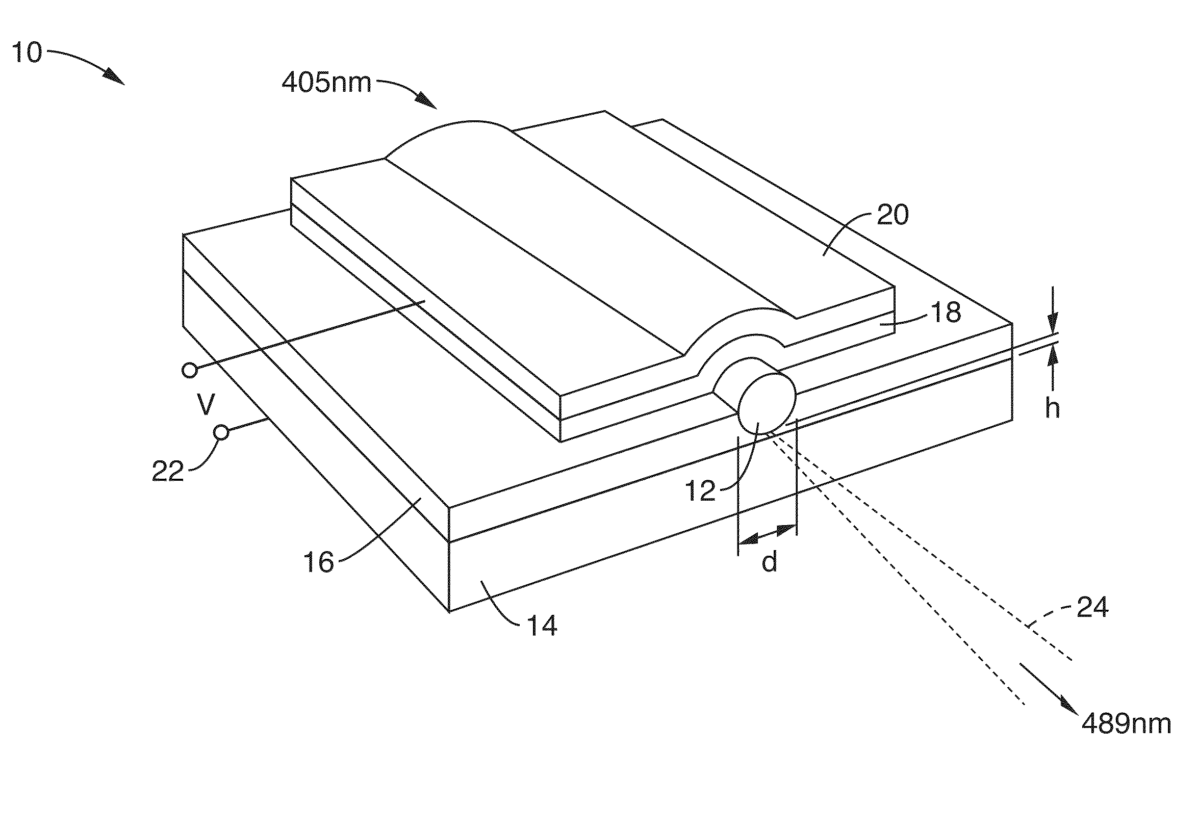
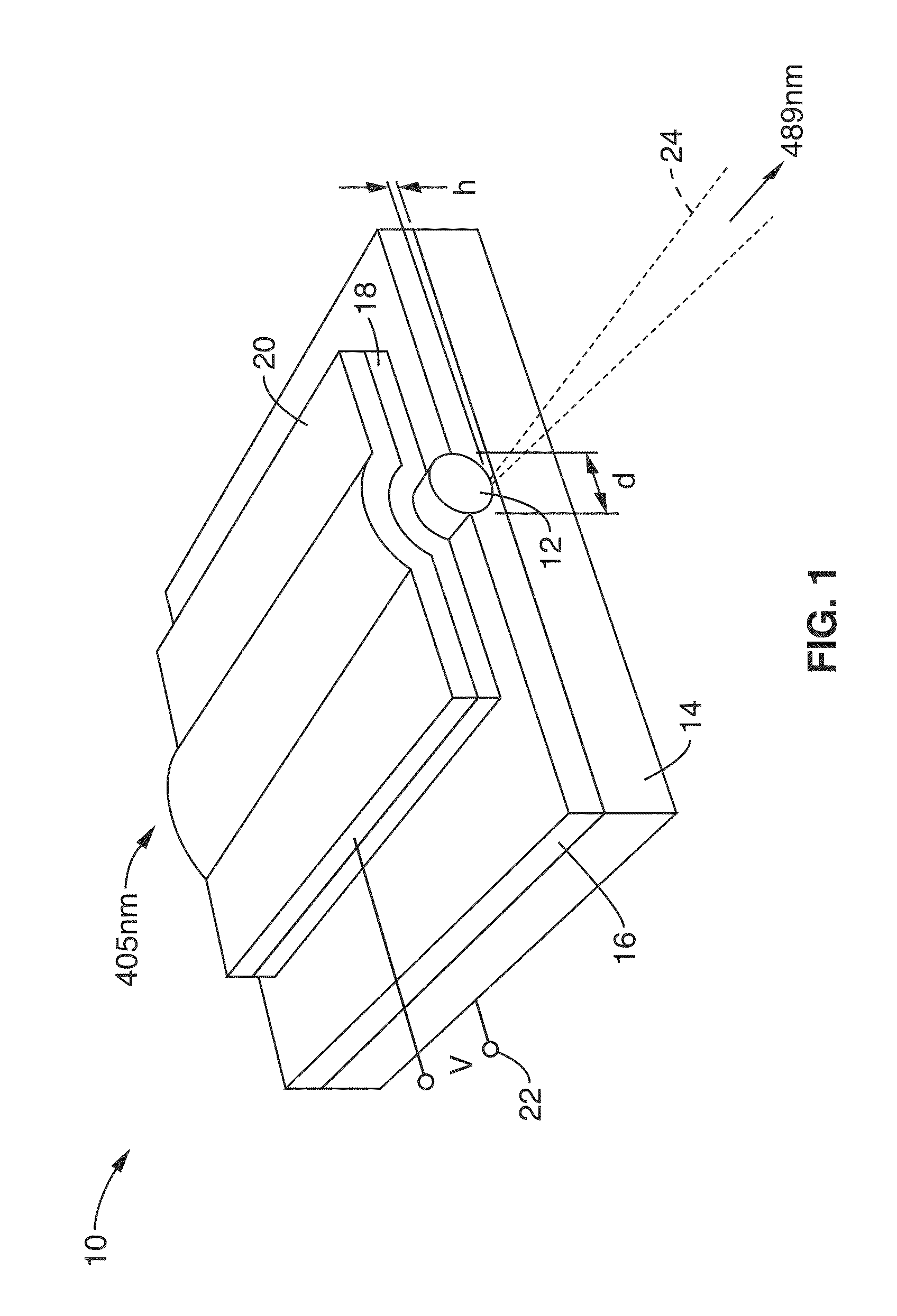
[0121]2. The laser source of embodiment 1, wherein at least a portion of the electron carrier population travel from the metal substrate through the low-refraction index gap to the semiconductor material.

[0122]3. The laser source of embodiment 1, wherein the laser source supports a plasmonic mode having a mode size smaller than λ / 2 in at least one dimension of the mode.

embodiment 3

[0123]4. The laser source of embodiment 3, wherein the laser source supports a plasmonic mode having a mode size smaller than λ / 20 in at least one dimension of the mode.

[0124]5. The laser source of embodiment 1, wherein the low-refraction index gap comprises a layer of material having a thickness that ranges between approximately 1 nm and approximately 100 nm.

embodiment 5

[0125]6. The laser source of embodiment 5, wherein the low-refraction index gap comprises a layer of material having a thickness that ranges between approximately 2 nm and approximately 50 nm.


PUM


Abstract

Hybrid plasmonic waveguides are described that employ a high-gain semiconductor nanostructure functioning as a gain medium that is separated from a metal substrate surface by a nanoscale thickness thick low-index gap. The waveguides are capable of efficient generation of sub-wavelength high intensity light and have the potential for large modulation bandwidth >1 THz.

Description

CROSS-REFERENCE TO RELATED APPLICATIONS[0001]This application is a 35 U.S.C. §111(a) continuation of PCT international application number PCT / US2011 / 045633 filed on Jul. 27, 2011, incorporated herein by reference in its entirety, which is a nonprovisional of U.S. provisional patent application Ser. No. 61 / 367,924 filed on Jul. 27, 2010, incorporated herein by reference in its entirety. Priority is claimed to each of the foregoing applications.[0002]The above-referenced PCT international application was published as PCT International Publication No. WO 2012 / 015990 on Feb. 2, 2012 and republished on Jun. 21, 2012, and is incorporated herein by reference in its entirety.STATEMENT REGARDING FEDERALLY SPONSORED RESEARCH OR DEVELOPMENT[0003]This invention was made with Government support under Grant No. 67N-1069929 awarded by the Air Force Office of Scientific Research (AFOSR) MURI and Grant No. CMMI-0751621 awarded by the National Science Foundation Nanoscale Science and Engineering Cent...

Claims


Application Information

Patent Timeline
Patent Type & Authority Patents(United States)
IPC IPC(8): H01S5/00
CPCH01S5/1046H01S5/2031B82Y20/00H01S5/341H01S5/30H01S5/0206H01S5/041H01S5/4031H01S5/22
Inventor ZHANG, XIANGSORGER, VOLKER JENDRIKOULTON, RUPERT FRANCIS MAXIMILLIANMA, REN-MIN
Owner RGT UNIV OF CALIFORNIA
Why Eureka
Try Eureka