Method for preparing silicon-based surface plasma waveguide having stepped structure

A surface plasmon, stepped structure technology, applied in the directions of light guide, optics, instrument, etc., can solve the problems of increased loss, limited efficiency and rate of third-order nonlinear effect, low speed of two-photon absorption, etc.

Inactive Publication Date: 2011-09-14
SHANGHAI JIAO TONG UNIV
View PDF1 Cites 7 Cited by
  • Summary
  • Abstract
  • Description
  • Claims
  • Application Information

AI Technical Summary

Problems solved by technology

But in this structure, when the effective mode field area is reduced to hundreds of square nanometers, the loss will increase sharply, which limits its nonlinear application.
[0005] The technology based on the silicon-on-insulator (SOI) structure makes it possible to integrate optoelectronic systems compatible with the CMOS process, but due to the moderate size of the third-order nonlinear coefficient of silicon, and the efficiency and speed of the third-order nonlinear effect are limited by double Photon Absorption and Low Velocity Free Carrier Absorption Effect

Method used


Image

  • Method for preparing silicon-based surface plasma waveguide having stepped structure
  • Method for preparing silicon-based surface plasma waveguide having stepped structure
  • Method for preparing silicon-based surface plasma waveguide having stepped structure

Examples


Embodiment

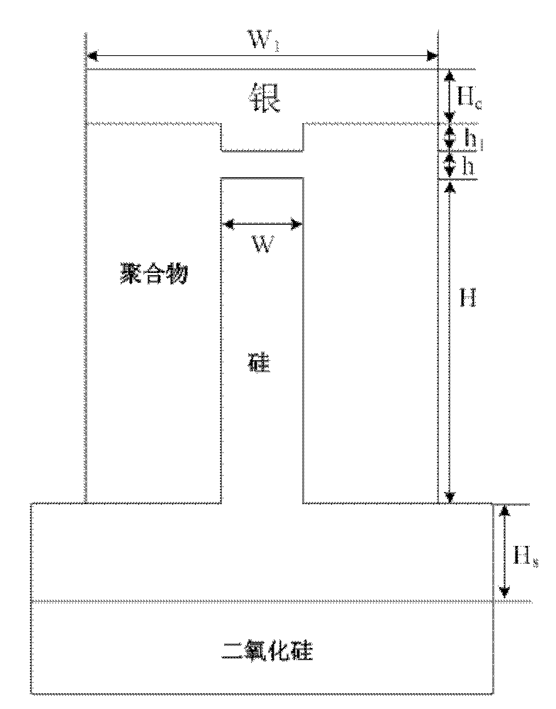
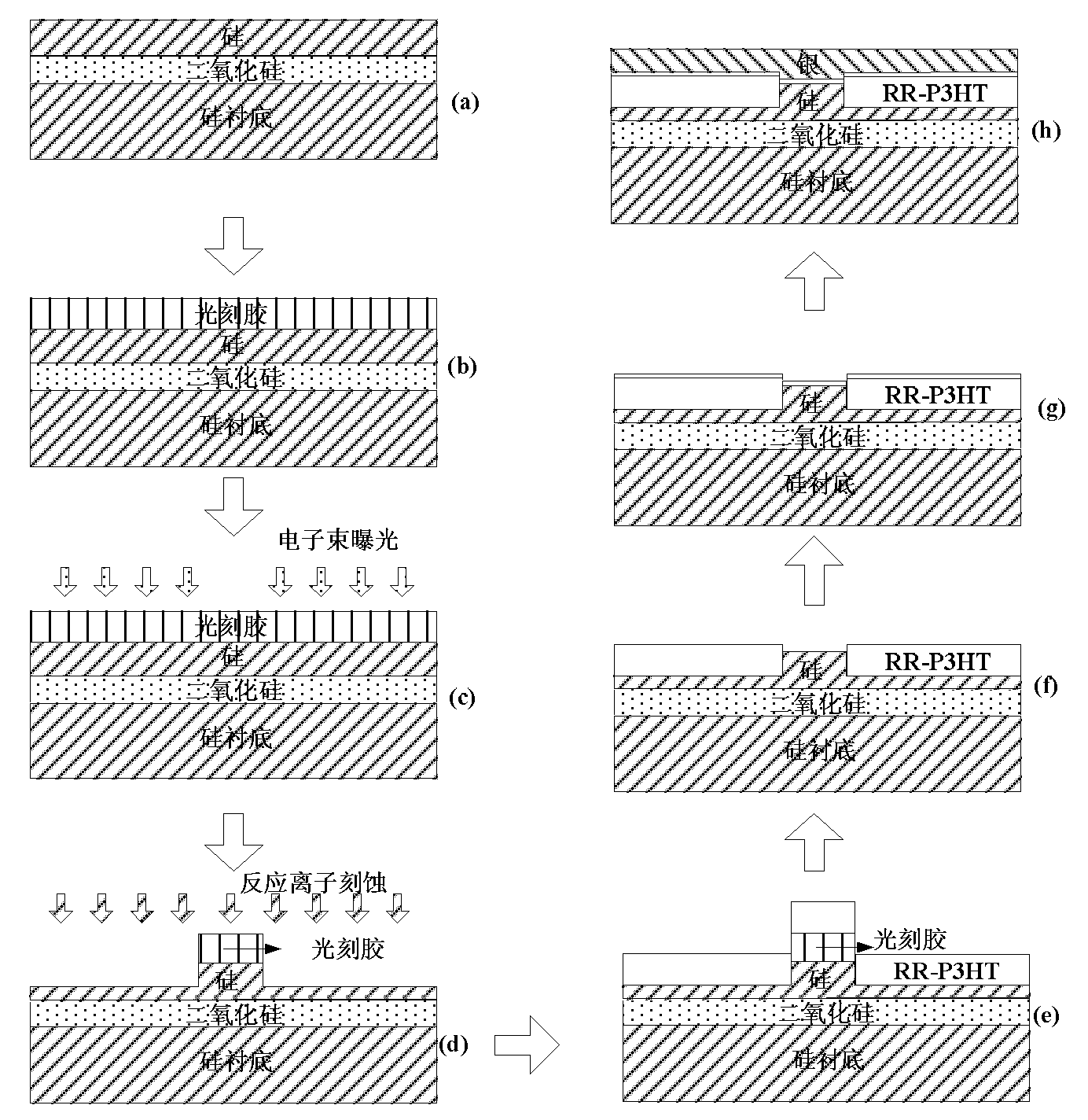
[0025] This embodiment includes the following steps:

[0026] The first step is to coat an electron beam photoresist on the SOI wafer, and then form a waveguide pattern on the silicon layer through an electron beam exposure (E-beam lithograph) system and a reactive ion etching (RIE) system;

[0027] The second step is to deposit a highly nonlinear polymer-regioregular poly-3-hexylthiophene (RR-P3HT) on the SOI ridge waveguide;

[0028] The deposition refers to: using the remaining electron beam photoresist after electron beam exposure as a mask to deposit RR-P3HT by molecular beam deposition;

[0029] The difference between the deposited thickness and the height of the SOI ridge waveguide is the step height of silver.

[0030] The third step is to remove the electron beam photoresist and RR-P3HT on it, and deposit RR-P3HT for the second time by molecular beam deposition

[0031] The thickness of the second deposition is 5nm.

[0032] The fourth step is to use the radio freq...


PUM


Abstract

The invention discloses a method for preparing a silicon-based surface plasma waveguide having a stepped structure in the technical field of nanometer semiconductors. The method comprises the following steps of: coating electron beam photoresist on a silicon-on-insulator (SOI) chip, and forming a waveguide pattern on a silicon layer through an electron beam exposure system and a reactive ion etching system; depositing high-nonlinearity polymer-regional regularity poly(3-hexylthiophene) on an SOI ridge waveguide; removing the electron beam photoresist and the high-nonlinearity polymer-regional regularity poly(3-hexylthiophene) thereon, and depositing the high-nonlinearity polymer-regional regularity poly(3-hexylthiophene) for the second time by a molecular beam deposition method; and plating metal silver on a polymer film by a radio frequency sputtering method, and preparing the silicon-based surface plasma waveguide having the stepped structure. The product has a nano-scale mode field and low transmission loss, and is combined with high-nonlinearity polymer materials to realize super-high nonlinearity.

Description

technical field [0001] The invention relates to a method in the field of nano-semiconductor technology, in particular to a method for preparing a silicon-based surface plasmon waveguide with a ladder structure. Background technique [0002] In recent years, nano-optics based on surface plasmon technology has received more and more attention. Surface plasmons break the diffraction limit of traditional dielectric waveguides, and can confine the light in the communication band to deep subwavelength waveguides, which can be like metal wires. Conduction electrons transport light at the nanometer scale, driving further reduction in device size and further increase in integration density. At the same time, as the chip gradually brings together multiple functions such as computing, storage, communication, and information processing, it promotes the realization of on-chip optical computing technology. In order to realize the logic and signal processing functions in optical computing...

Claims


Application Information

Patent Timeline
Patent Type & Authority Applications(China)
IPC IPC(8): G02B6/136G02B6/132G02B6/122
Inventor 周淦胡小锋张亮苏翼凯
Owner SHANGHAI JIAO TONG UNIV
Why Eureka
Try Eureka