
Terahertz emission source based on transition metal chalcogenide and excitation method

A technology of chalcogenides and transition metals, applied in the field of terahertz band devices, can solve the problems of inability to effectively radiate elliptically polarized terahertz waves, terahertz signal noise, etc., to improve mobility and nonlinear coefficient, and stabilize lattice structure, the effect of improving the modulation efficiency

Inactive Publication Date: 2018-11-30
NORTHWEST UNIV
View PDF4 Cites 8 Cited by
  • Summary
  • Abstract
  • Description
  • Claims
  • Application Information

AI Technical Summary

Problems solved by technology

[0004] In view of the defects and deficiencies of the prior art, the purpose of the present invention is to provide a transition metal chalcogenide-based terahertz emission source and excitation method, which solves the problem that the terahertz signal excited by the existing terahertz emission source has noise and cannot effectively The problem of radiating elliptically polarized terahertz waves

Method used


Image

  • Terahertz emission source based on transition metal chalcogenide and excitation method
  • Terahertz emission source based on transition metal chalcogenide and excitation method
  • Terahertz emission source based on transition metal chalcogenide and excitation method

Examples


Embodiment 1

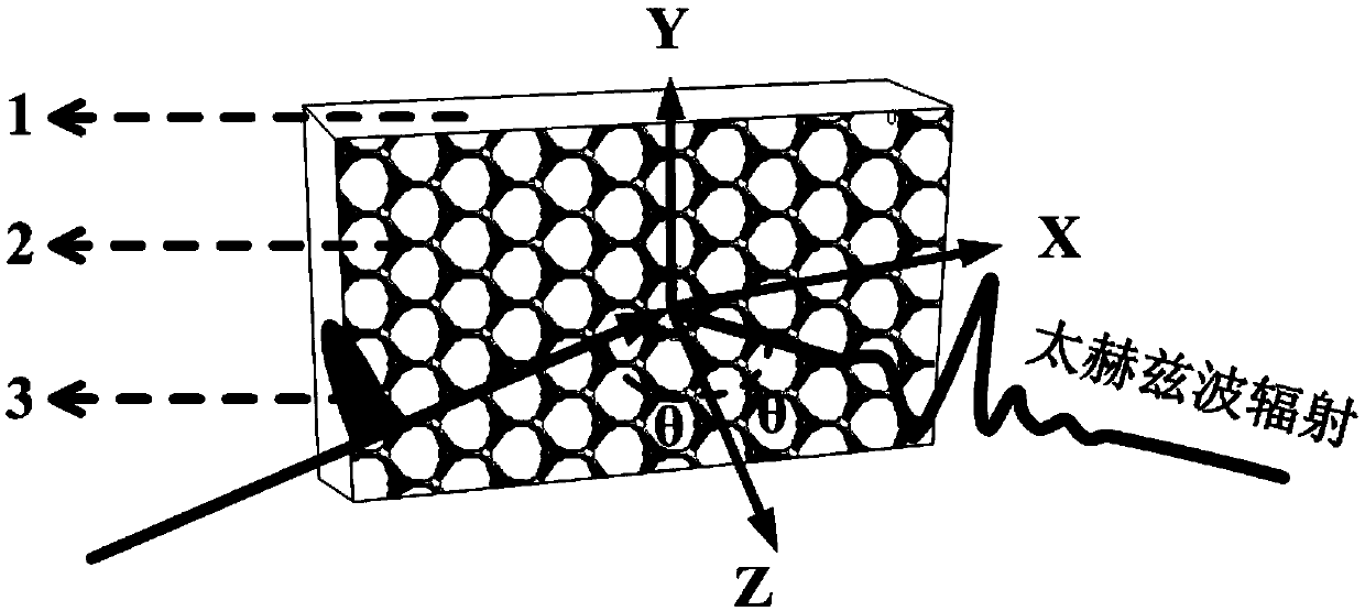
[0045] Such as figure 1 As shown, the terahertz emission source of this embodiment includes a quartz substrate 1 and a tungsten disulfide crystal thin film layer 2, the thickness of the thin film layer is 100nm, a femtosecond laser with a frequency of 800nm, a pulse width of 60fs, and a repetition rate of 1KHz is used as the pumping light source 3. In this embodiment, the pump power is 0.42~2.00mJ / cm 2 ,, the femtosecond laser pulse pumps and excites the surface of the radiation device at a 45° oblique incidence, and detects the terahertz wave radiation at the 45° reflective surface. Using zinc telluride as the detection crystal to detect terahertz waves on the 45° reflective surface, the results are as follows Figure 4 (a) shown.

[0046] The signal-to-noise ratio of the terahertz wave radiation obtained in this example is -18.4--37.4dB in the range of 0.58-2.5THz, and the electron mobility is 50-150cm 2 V -1 S -1 , The radiation electric field strength is 0.22-0.51kV / c...

Embodiment 2

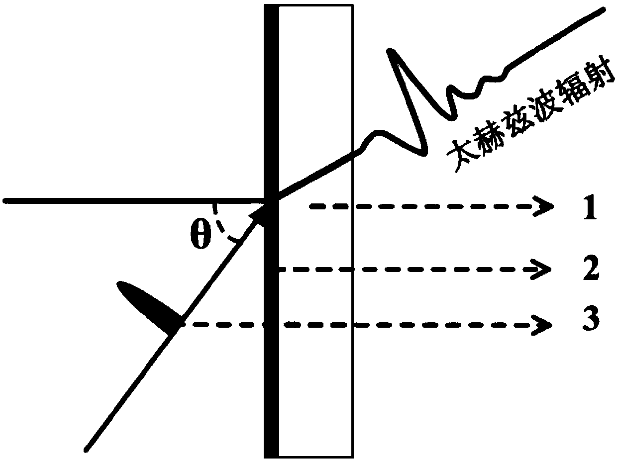
[0048] Such as figure 2 As shown, the terahertz emission source of this embodiment includes a quartz substrate 1 and a tungsten disulfide thin film layer 2, the thickness of the thin film layer is 0.72nm, and a femtosecond laser with a frequency of 800nm, a pulse width of 60fs, and a repetition rate of 1KHz is used as the pumping light source 3. Among them, the pump power is 4.53~6.51mJ / cm 2 . The femtosecond laser pulse is incident at 45° obliquely to pump and excite the surface of the radiation device, and detect the terahertz wave radiation at 45° in the transmission path, and detect the terahertz wave radiation on the 45° transmission surface, the results are as follows Figure 4 (b) shown.

[0049] The signal-to-noise ratio of the terahertz wave radiation obtained in this example is -17.6--34.9dB in the range of 0.58-2.5THz, and the electron mobility is 150-200cm 2 V -1 S -1 , The radiation electric field strength is 0.11 ~ 0.26kV / cm.

Embodiment 3

[0051] The difference between this embodiment and embodiment 2 lies in that the thickness of the film layer is 8nm. It is found that the film layer in this embodiment can radiate elliptically polarized terahertz waves.


PUM

PropertyMeasurementUnit
Thicknessaaaaaaaaaa
Thicknessaaaaaaaaaa
Center frequencyaaaaaaaaaa

Abstract

The invention discloses a terahertz emission source based on transition metal chalcogenide and an excitation method. The terahertz emission source comprises a transition metal chalcogenide film and pumping light source. The terahertz emission source has the advantages that fixed incoming excitation pulses are used, the planar central axis of the transition metal chalcogenide film is rotated, and pumping light source laser comes in at 0-90 degrees and excite the surface of the transition metal chalcogenide film to radiate terahertz waves; the transition metal chalcogenide film is used as the terahertz emission source, so that the generated terahertz emission source is high in radiation efficiency; in addition, due to the fact that the film is good in heat conductivity, stable in lattice structure and adjustable in energy band gap, device service life and wide application range are guaranteed, and a two-dimensional terahertz emission source type gap is filled up; by using the transitionmetal chalcogenide film as the terahertz emission source, elliptical polarization terahertz waves can be generated, and the elliptical polarization terahertz waves is significant in molecular chirality spectrum, substance circular dichroism spectrum, polarization imaging and the like.

Description

technical field [0001] The invention belongs to the technical field of terahertz band devices, and in particular relates to a transition metal chalcogenide-based terahertz emission source and an excitation method. Background technique [0002] Terahertz waves generally refer to electromagnetic waves ranging from 0.1 THz to 10 THz, with wavelengths ranging from 30 μm to 3 mm. Overlapping between microwave and far-infrared, it is in the transition zone from electronics to photonics. It has excellent properties such as low photon energy, non-polar substance penetration and molecular fingerprint spectrum. It is used in biomedicine, safety monitoring, and material identification. Fields have very large potential value. In the early days, due to the lack of efficient terahertz sources, high-sensitivity detectors and terahertz-related functional devices, the development of terahertz technology was hindered, which was once called "terahertz gap". With the development and maturity ...

Claims


Application Information

Patent Timeline
IPC IPC(8): G02F1/35G02F1/355H01S3/00
CPCG02F1/3501G02F1/3551H01S3/00
Inventor 徐新龙张隆辉姚泽瀚黄媛媛朱礼鹏卢春辉
Owner NORTHWEST UNIV
Learn More