Hybrid Coupling Structure of the short Range Plasmon Polariton and Conventional Dielectric Waveguide, A Coupling Structure of the Long Range Plasmon Polariton and Conventional Dielectric Waveguide, and Applications Thereof

a technology of plasmon polariton and dielectric waveguide, applied in the field of photoelectron technique, can solve the problems of low detection sensitivity, inferior stability, and change in output power

Active Publication Date: 2010-12-09
ROHM CO LTD +1
View PDF9 Cites 8 Cited by
  • Summary
  • Abstract
  • Description
  • Claims
  • Application Information

AI Technical Summary

Problems solved by technology

However, a wave field of a the short range SPP wave approximates a metal surface at a higher degree as compared with a conventional SPP wave and a mode characteristic thereof is extremely sensitive to a refractive index change in a dielectric in an ultrathin range around a metal film, and hence an obvious change is caused in the coupling of a short range surface plasmon polariton mode and a conventional dielectric waveguide mode and a drastic change in output power of the dielectric waveguide is caused if the refractive i

Method used


Image

  • Hybrid Coupling Structure of the short Range Plasmon Polariton and Conventional Dielectric Waveguide, A Coupling Structure of the Long Range Plasmon Polariton and Conventional Dielectric Waveguide, and Applications Thereof
  • Hybrid Coupling Structure of the short Range Plasmon Polariton and Conventional Dielectric Waveguide, A Coupling Structure of the Long Range Plasmon Polariton and Conventional Dielectric Waveguide, and Applications Thereof
  • Hybrid Coupling Structure of the short Range Plasmon Polariton and Conventional Dielectric Waveguide, A Coupling Structure of the Long Range Plasmon Polariton and Conventional Dielectric Waveguide, and Applications Thereof

Examples


example 1

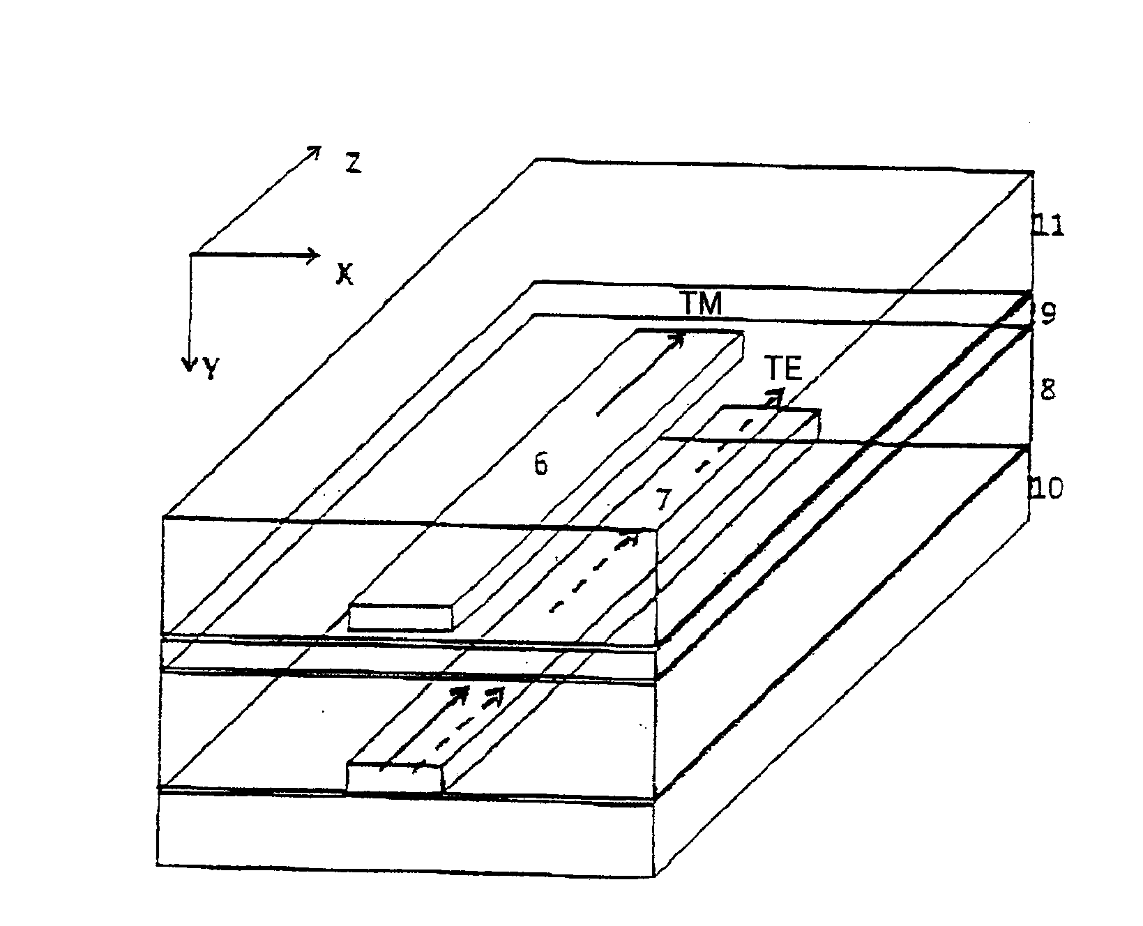
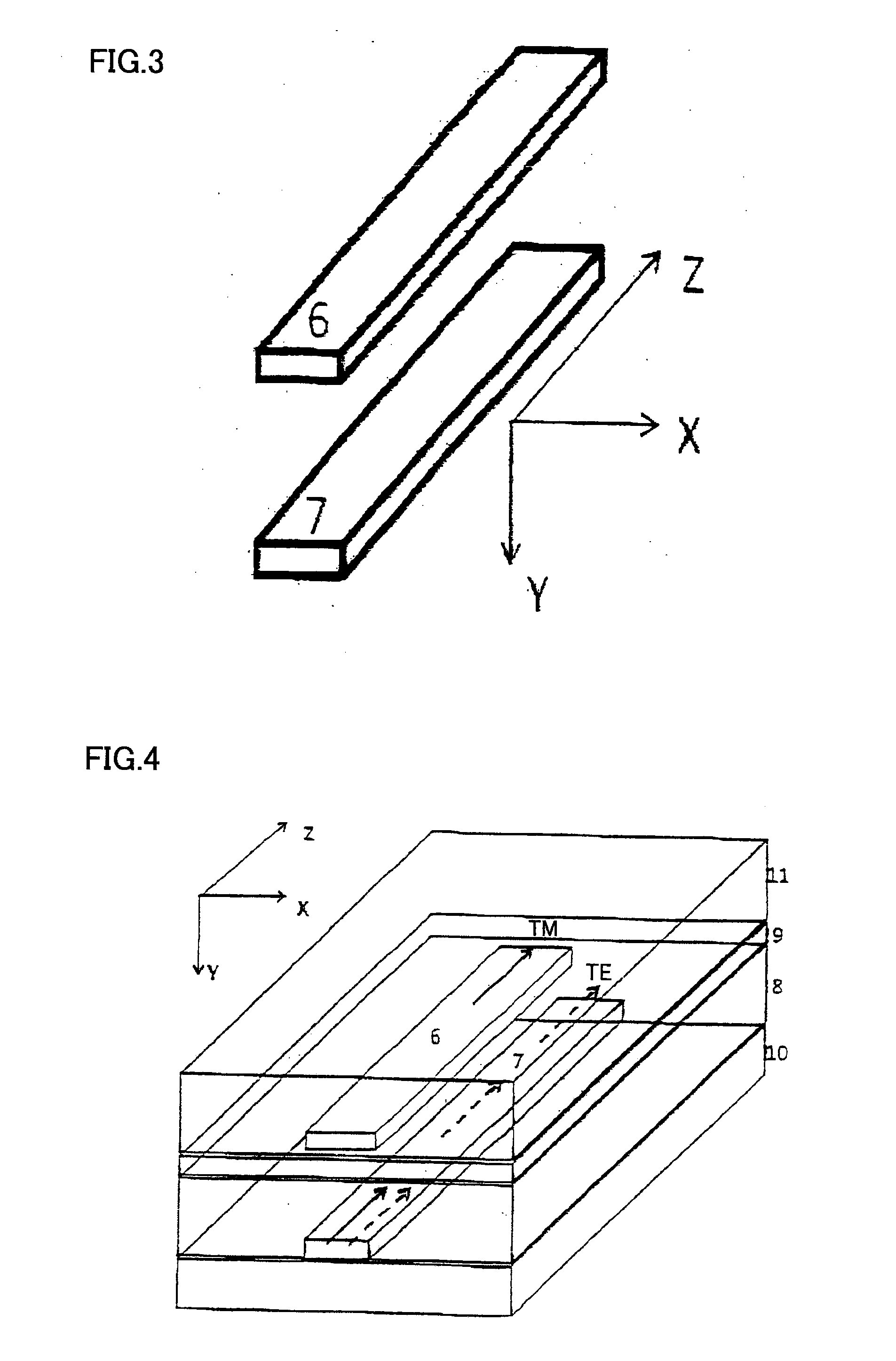
[0120]As to the coupling structure of the long range surface plasmon polariton and the dielectric waveguide provided by the present invention, this structure includes a dielectric substrate layer 10, a dielectric waveguide layer 7, a coupling matching layer 8, and a long range surface plasmon waveguide portion, formed on the coupling matching layer, for conducting the long range surface plasmon polariton, upward from below, as shown in FIGS. 16 and 17.

[0121]The refractive index of dielectric waveguide layer 7 is larger than the refractive index of dielectric substrate layer 10, and larger than the refractive index of coupling matching layer 8. Selection of the refractive index of dielectric waveguide layer 7 equalizes or relatively approximates the equivalent refractive index of a TM polarization base mode of the dielectric waveguide with or to the equivalent refractive index of the long range surface plasmon polariton. Preferably, the refractive index of dielectric waveguide layer ...

example 2

[0126]Shown in FIGS. 18 and 19 are structural diagrams of a refractive index sensor to which the coupling structure of the long range surface plasmon polariton and the dielectric waveguide according to the present invention is applied, and the refractive index sensor is mainly constituted of the aforementioned coupling structure. The material for a dielectric substrate layer 10 is SiO2, a dielectric waveguide layer 7 formed on dielectric substrate layer 10 by ultraviolet photoetching and chemical vapor deposition is an Si3N4 strip having a width of 2 μm and a thickness of 220 nm, both of a coupling matching layer 8 and a dielectric buffer layer 9 are made of SiO2 having a refractive index of 1.45 with a total thickness of 6 μm, and a metal layer 6 prepared by ultraviolet photoetching and sputtering is an Al strip having a width of 5 μm, a length of 640 μm and a thickness of 25 nm.

[0127]Above metal layer 6 is a measured object, i.e., the dielectric cover layer, and when the refractiv...

example 3

[0130]Shown in FIGS. 18 and 19 are structural diagrams of a refractive index sensor to which the coupling structure of the long range surface plasmon polariton and the dielectric waveguide according to the present invention is applied, and the refractive index sensor is mainly constituted of the aforementioned coupling structure. The material for a dielectric substrate layer 10 is SiO2, a dielectric waveguide layer 7 formed on the substrate by ultraviolet photoetching and chemical vapor deposition is an Si3N4 strip having a width of 5 μm and a thickness of 120 nm, a coupling matching layer 8 is SiO2 having a thickness of 3 μm, a dielectric buffer layer 9 is a CYTOP resin layer having a thickness of 4 μm and a refractive index of 1.38, and a metal layer 6 is an Au strip having a width of 20 μm, a length of 1050 μm and a thickness of 30 nm.

[0131]When the refractive index of a dielectric cover layer 11 above metal layer 6 changes following physical (temperature, humidity, pressure, ele...


PUM


Abstract

The present invention provides a hybrid coupling structure of a short range surface plasmon polariton and a conventional dielectric waveguide, including a dielectric substrate layer, a dielectric waveguide layer positioned on the said dielectric substrate layer, a coupling matching layer positioned on the said dielectric waveguide layer and a short range surface plasmon waveguide portion, formed on the said coupling matching layer, for conducting the short range surface plasmon polariton. The present invention also provides a coupling structure of a long range surface plasmon polariton and a dielectric waveguide, including a dielectric substrate layer, a dielectric waveguide layer, a coupling matching layer and a long range surface plasmon waveguide portion upward from below respectively.

Description

BACKGROUND OF THE INVENTION[0001]1. Field of the Invention[0002]The present invention relates to the field of the photoelectron technique, and more specifically, it relates to a hybrid coupling structure of a short range surface plasmon polariton and a conventional dielectric waveguide and a coupling structure of a long range surface plasmon polariton and a dielectric waveguide, as well as a refractive index sensor, a TM polarization modulator etc. based on the structures.[0003]2. Description of the Background Art[0004]A surface plasmon polariton (SPP) is an electromagnetic field propagating along the interface between a metal and a dielectric. As shown in FIG. 1, 1 denotes a metal (or a mixture of a metal and a dielectric), 2 denotes dielectrics around the metal and numeral 3 denotes surface plasmon polaritons on interfacial portions, and coupling develops in the SPPs on the upper and lower surfaces when the metal is sufficiently thin, to form a symmetric mode, i.e., a long range s...

Claims


Application Information

Patent Timeline
IPC IPC(8): G02B6/26G02F1/01
CPCB82Y20/00G01N21/43G01N21/553G02F2203/10G02B6/1226G02F1/035G02F2001/0144G01N21/7703G02F1/0144
Inventor LIU, FANWAN, RUI-YUANHUANG, YI-DONGFENG, XUEZHANG, WEIPENG, JIANG DEMIURA, YOSHIKATSUNIWA, DAISUKEOHNISHI, DAI
Owner ROHM CO LTD
Why Eureka
Try Eureka