Wedge-type surface plasma waveguide

A surface plasmon and waveguide technology, applied in the field of nanophotonics, can solve the problems of adjacent channel crosstalk, large mode field area, increase device size, etc. Effect

Inactive Publication Date: 2014-07-30
GUILIN UNIV OF ELECTRONIC TECH
View PDF2 Cites 7 Cited by
  • Summary
  • Abstract
  • Description
  • Claims
  • Application Information

AI Technical Summary

Problems solved by technology

The advantage of the single-wedge surface plasmon waveguide is that it can confine the energy to the apex of the triangular wedge, but its one-sided pursuit of propagation distance ignores the effective mode field area, which eventuall

Method used


Image

  • Wedge-type surface plasma waveguide

Examples


Embodiment Construction

[0020] The present invention will be described in further detail below in conjunction with the accompanying drawings and embodiments.

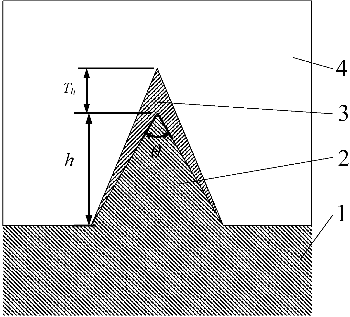
[0021] Embodiments of the wedge-shaped surface plasmon waveguide such as figure 1 As shown, the metal base 1 and the metal wedge 2 on it are made of metallic silver, and the relative permittivity ε metal =-129+3.3i, dielectric layer 2 is silicon dioxide, relative permittivity ε d =2.25, the relative permittivity ε of the vacuum environment air =1. The height h=2 μm of the tip of the metal wedge 2 of this example, the tip angle θ=40° of the metal wedge 2, the two base angles of this example are equal, and can also be unequal acute angles. The thickness of the dielectric layer 3 attached to the tip of the metal wedge is T h = 5nm, the dielectric layer 3 is attached to both sides of the metal wedge 2, and the dielectric layer 3 is gradually thinned from top to bottom until the thickness of the dielectric layer on the surface of the metal base...


PUM


Abstract

The invention discloses a wedge-type surface plasma waveguide. The wedge-type surface plasma waveguide comprises a metal substrate and a metal wedge, wherein the metal substrate is made of low-loss metal materials; the metal wedge is arranged on the metal substrate; the cross section of the metal wedge is triangular; a dielectric layer is attached to the sharp end of the metal wedge. The exterior of the dielectric layer is surrounded by a vacuum. The three angles of the triangle of the cross section of the metal wedge are acute angles. The dielectric layer is silicon dioxide or magnesium fluoride. The two side faces and the outer surface, attached to the metal wedge, of the dielectric layer are planes which are thinned gradually from top to bottom. Compared with a single wedge-type surface plasma waveguide under the same conditions, the wedge-type surface plasma waveguide has the advantages that the ratio of the propagation distance of surface plasma wave to the effective mode field area is effectively increased, and the final quality factor is increased by one order of magnitude; the light guide function of the surface plasma waveguide is achieved, the crosstalk between channels is effectively reduced, microminiaturization of a photon circuit is facilitated, and the integration is improved; the waveguide is simple in structure and easy to implement.

Description

technical field [0001] The invention belongs to a waveguide in the field of nanophotonics, in particular to a wedge-shaped surface plasmon waveguide. Background technique [0002] In recent years, the development of traditional dielectric integrated optical devices has been limited by the diffraction limit, and the miniaturization and integration have encountered bottlenecks, but surface plasmon waves can limit light to nanometer dimensions. Therefore, using surface plasmon waves to achieve sub-wavelength Devices have become a research hotspot. [0003] Surface plasmon waves are slow waves, which have a larger phase velocity, shorter wavelength, higher momentum, and higher wave impedance than conventional media waves. However, the dielectric constant of metals is negative in the light wave band , its imaginary part represents the ability of the metal to absorb light. This structure is at the cost of loss. Its restriction and loss are a pair of eternal contradictions. The st...

Claims


Application Information

Patent Timeline
IPC IPC(8): G02B6/122
Inventor 陈明童秀倩李海鸥尚军萍陈辉
Owner GUILIN UNIV OF ELECTRONIC TECH
Why Eureka
Try Eureka