Chemical mechanical polishing aqueous dispersion and chemical mechanical polishing method for semiconductor device

a chemical mechanical and semiconductor technology, applied in lapping machines, other chemical processes, manufacturing tools, etc., can solve the problems of incomplete copper removal, large friction, and large reduction of polishing rate, so as to reduce copper dishing and copper corrosion, reduce friction during polishing, and high affinity to copper

Inactive Publication Date: 2014-01-09
JSR CORPORATIOON
View PDF0 Cites 2 Cited by
  • Summary
  • Abstract
  • Description
  • Claims
  • Application Information

AI Technical Summary

Benefits of technology

The present invention relates to a chemical mechanical polishing aqueous dispersion that can effectively polish copper without causing copper dishing or corrosion. The dispersion includes a first water-soluble polymer having a specific molecular weight and a heterocyclic ring in its molecule, a second water-soluble polymer or its salt having a specific molecular weight and a carboxyl or sulfonic group, an oxidizing agent, and abrasive grains. The dispersion has a pH of 7 to 12. The use of the first water-soluble polymer reduces friction during polishing and protects copper interconnects. The second water-soluble polymer or its salt increases the viscosity of the dispersion to prevent fangs and scratches. The dispersion has a viscosity of less than 2 mPa·s to prevent non-uniformity in polishing and dishing.

Problems solved by technology

When using a low-dielectric-constant material (low-k material) for an insulating layer, since delamination or layer breakage occurs when friction occurs to a large extent during polishing, it is difficult to apply a chemical mechanical polishing aqueous dispersion which causes friction to occur to a large extent during polishing.
On the other hand, since the water-soluble polymer also adheres to the polishing target area, the polishing rate decreases to a large extent, whereby incomplete copper removal or the like occurs.

Method used


Image

  • Chemical mechanical polishing aqueous dispersion and chemical mechanical polishing method for semiconductor device
  • Chemical mechanical polishing aqueous dispersion and chemical mechanical polishing method for semiconductor device
  • Chemical mechanical polishing aqueous dispersion and chemical mechanical polishing method for semiconductor device

Examples


first specific example

2.1 First Specific Example

2.1.1 Polishing Target

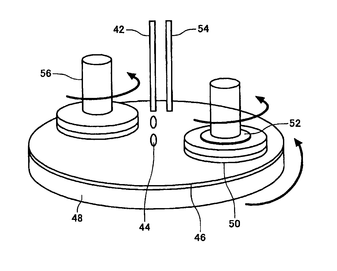
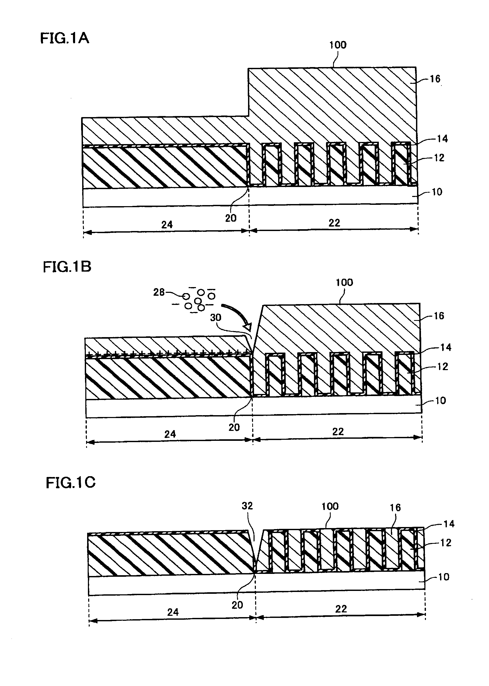
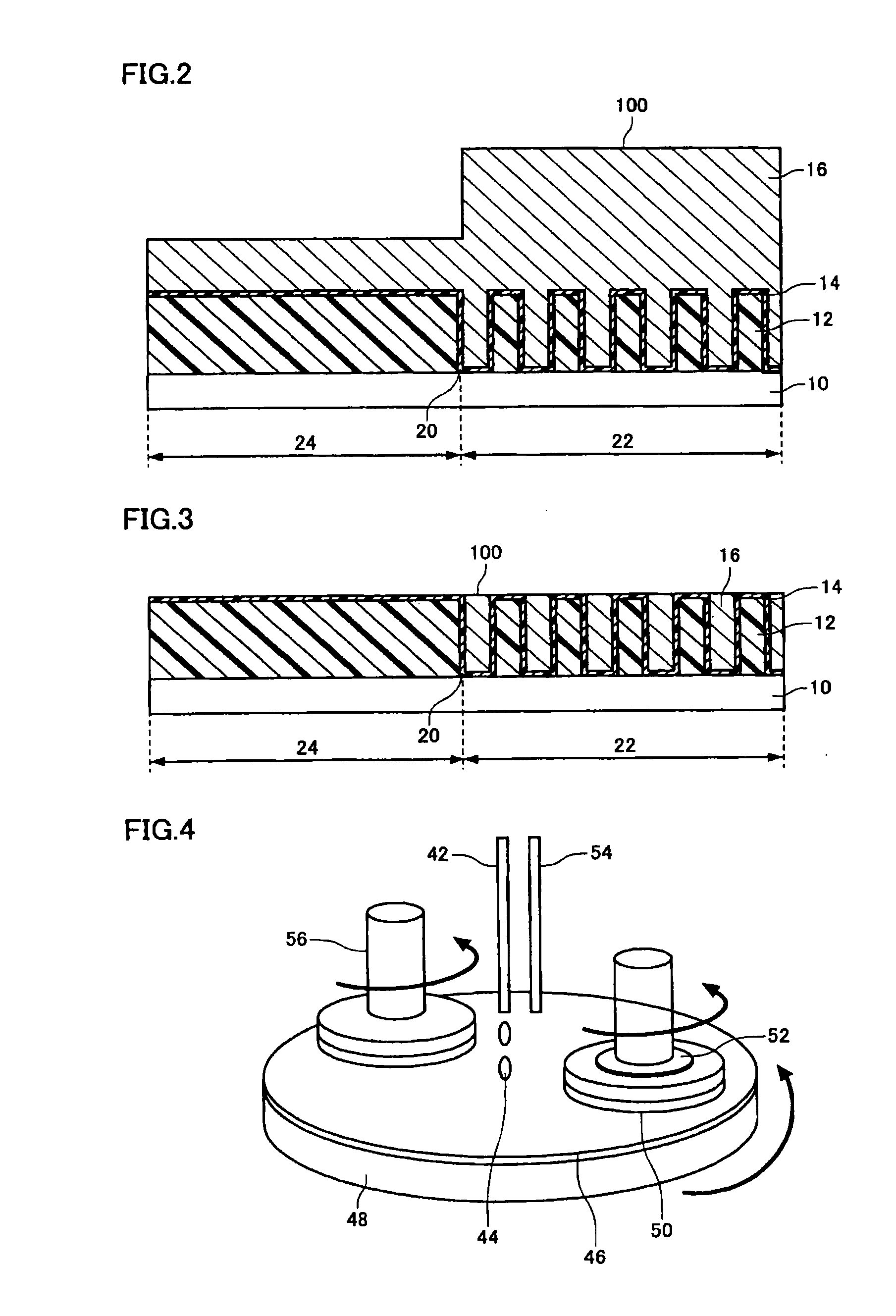
[0101]FIG. 2 shows a polishing target 100 of the chemical mechanical polishing method according to a first specific example. FIG. 2 shows a polishing target which is the same as that shown in FIG. 1A. The material for each layer and the like are also described below.

[0102]An insulating layer 12 formed of silicon oxide is provided on a substrate 10 on which semiconductor elements (not shown) are formed. An interconnect depression 20 is formed by etching the insulating layer 12. The insulating layer 12 may be a PETEOS layer, an insulating layer having a relative dielectric constant of 3.5 or less, or the like. The insulating layer 12 is preferably an insulating layer having a relative dielectric constant of 3.5 or less, and more preferably 3.0 or less.

[0103]A barrier layer 14 is formed to cover the surface of the insulating layer 12 and the bottom and the inner wall surface of the interconnect depression 20. The barrier layer 14 may be f...


PUM

PropertyMeasurementUnit
weight average molecular weightaaaaaaaaaa
viscosityaaaaaaaaaa
viscosityaaaaaaaaaa

Abstract

A chemical mechanical polishing aqueous dispersion of the invention includes (A) a first water-soluble polymer having a weight average molecular weight of 500,000 to 2,000,000 and including a heterocyclic ring in its molecule, (B) a second water-soluble polymer or its salt having a weight average molecular weight of 1000 to 10,000 and including one group selected from a carboxyl group and a sulfonic group, (C) an oxidizing agent, and (D) abrasive grains, and has a pH of 7 to 12.

Description

TECHNICAL FIELD[0001]The present invention relates to a chemical mechanical polishing aqueous dispersion suitably used when producing a semiconductor device, and a chemical mechanical polishing method using the chemical mechanical polishing aqueous dispersion.BACKGROUND ART[0002]In recent years, interconnects formed in semiconductor devices have been increasingly scaled down along with an increase in the degree of integration (density) of semiconductor devices. A damascene method has been known as technology capable of scaling down interconnects. In the damascene method, grooves or the like formed in an insulating layer are filled with an interconnect material, and an unnecessary interconnect material deposited in an area other than the grooves is removed by chemical mechanical polishing to form desired interconnects. When using copper or a copper alloy as an interconnect material, a high-strength, high-dielectric-constant insulating layer (barrier layer) is generally formed of tant...

Claims


Application Information

Patent Timeline
Patent Type & Authority Applications(United States)
IPC IPC(8): H01L21/306C09G1/02B24B37/00C09K3/14H01L21/304
CPCH01L21/30625C09G1/02C09K3/1463H01L21/3212C09K3/14H01L21/304B24B37/00
Inventor NAMIE, YUUJIKONNO, TOMOHISAMOTONARI, MASAYUKISHIDA, HIROTAKATAKEMURA, AKIHIRO
Owner JSR CORPORATIOON
Why Eureka
Try Eureka