Wafer-level device packaging

a technology of device packaging and wafers, applied in semiconductor devices, semiconductor/solid-state device details, electrical devices, etc., can solve the problems of increasing stringentness, increasing the complexity of package designs, and tsv and shell case approaches that require expensive wafer processing, and achieves low cost, reliable interconnection, and thin package profile

Active Publication Date: 2014-01-23
HONG KONG APPLIED SCI & TECH RES INST
View PDF22 Cites 8 Cited by
  • Summary
  • Abstract
  • Description
  • Claims
  • Application Information

AI Technical Summary

Benefits of technology

[0010]In one embodiment, an image sensor package is formed which is vertically integrated with a digital signal processor and memory chip along with lenses and a protective cover. Low cost and reliable interconnects are formed and a thinner package profile is enabled by the present invention.

Problems solved by technology

Packaging requirements for semiconductor devices have become more stringent as the competing demands of increased functionality and smaller electronic products continue to force device manufacturers to create ever more complex package designs.
Both the TSV and SHELLCASE approaches require expensive wafer processing to create the final multi-chip device package.
Further, the SHELLCASE approach requires a complex electrical path which can lead to decreased package reliability, particularly in view of the large differences in coefficients of thermal expansion between metallization layers and underlying semiconductor materials.

Method used


Image

  • Wafer-level device packaging
  • Wafer-level device packaging
  • Wafer-level device packaging

Examples


Embodiment Construction

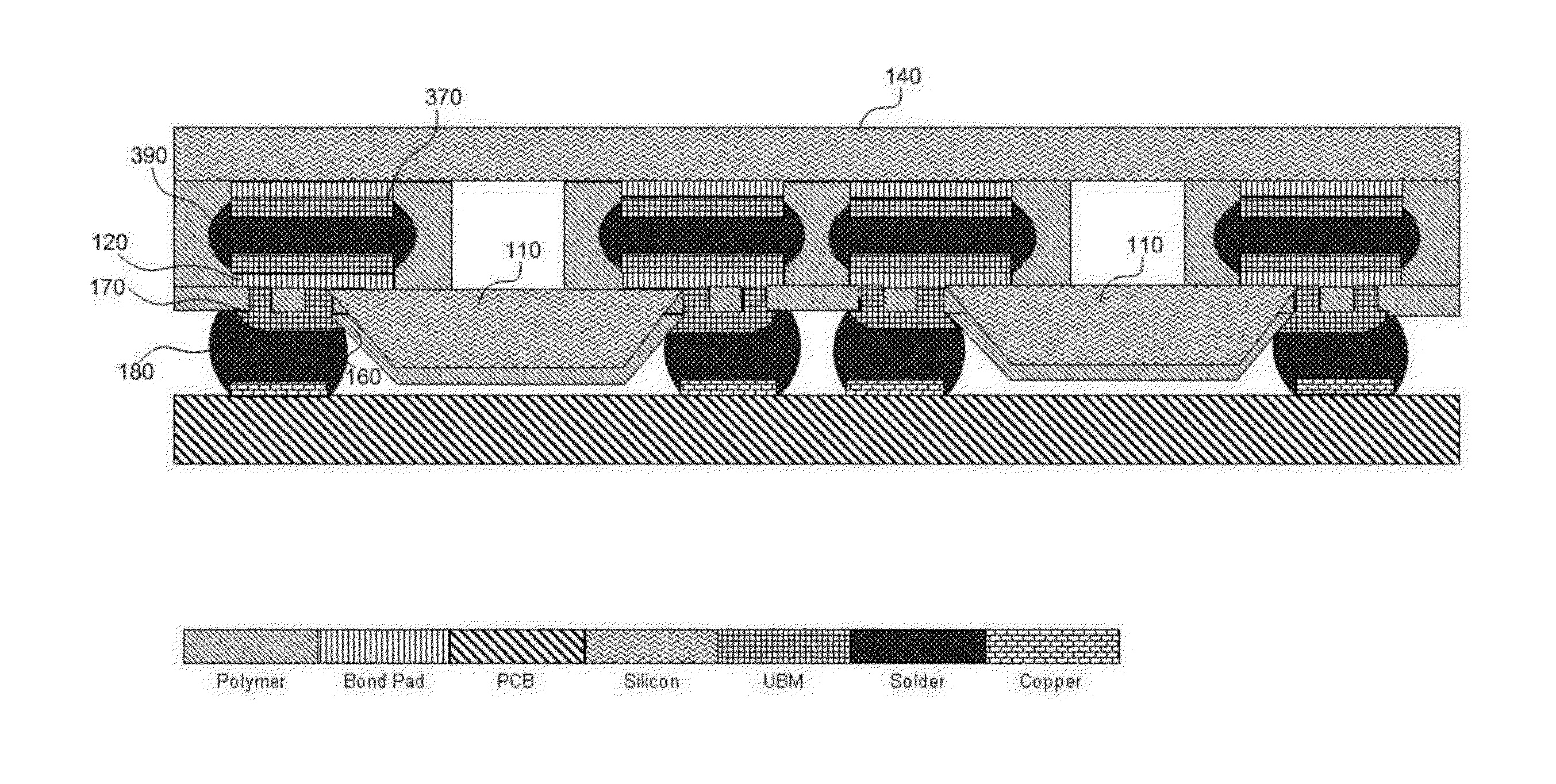
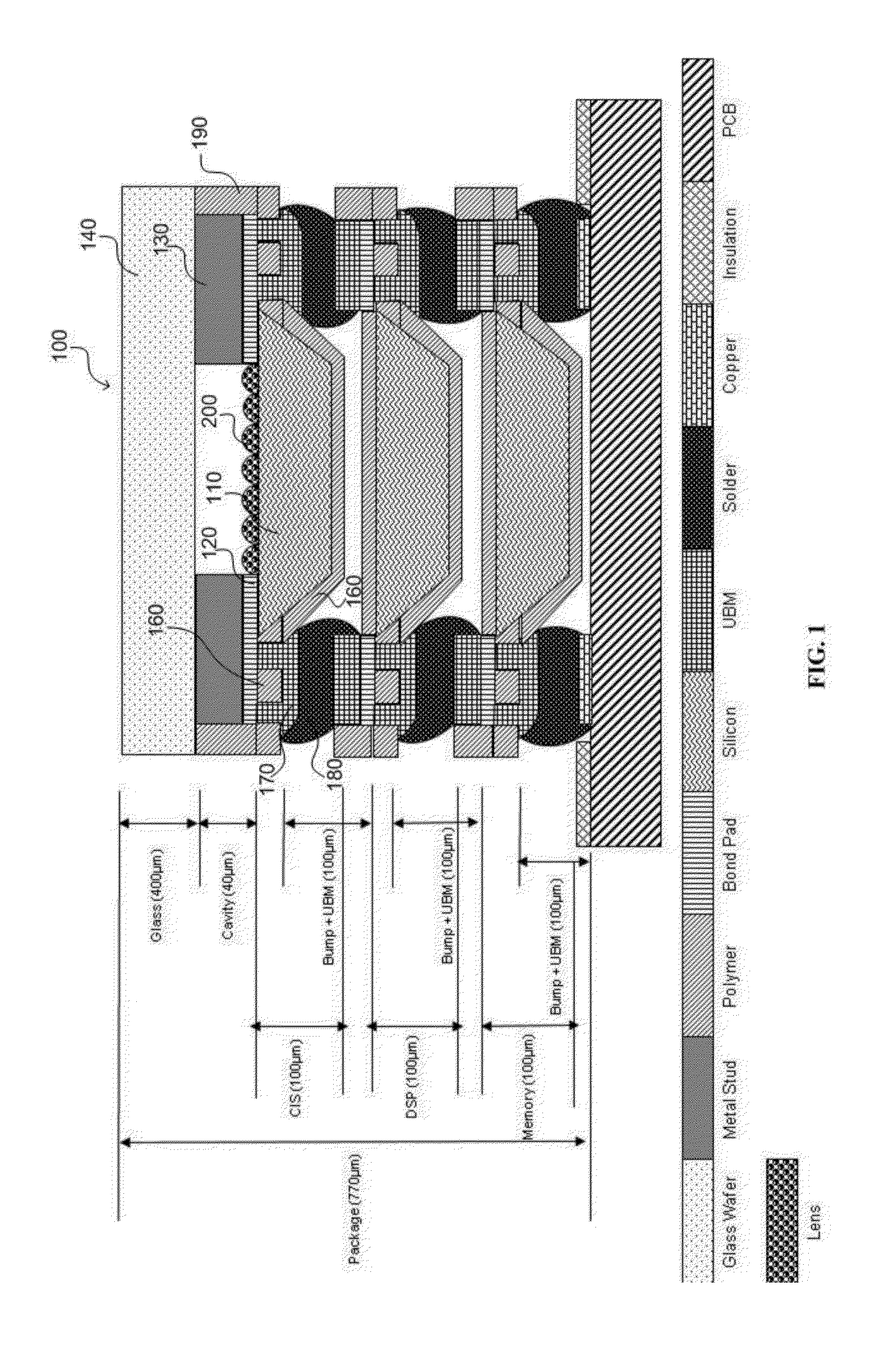
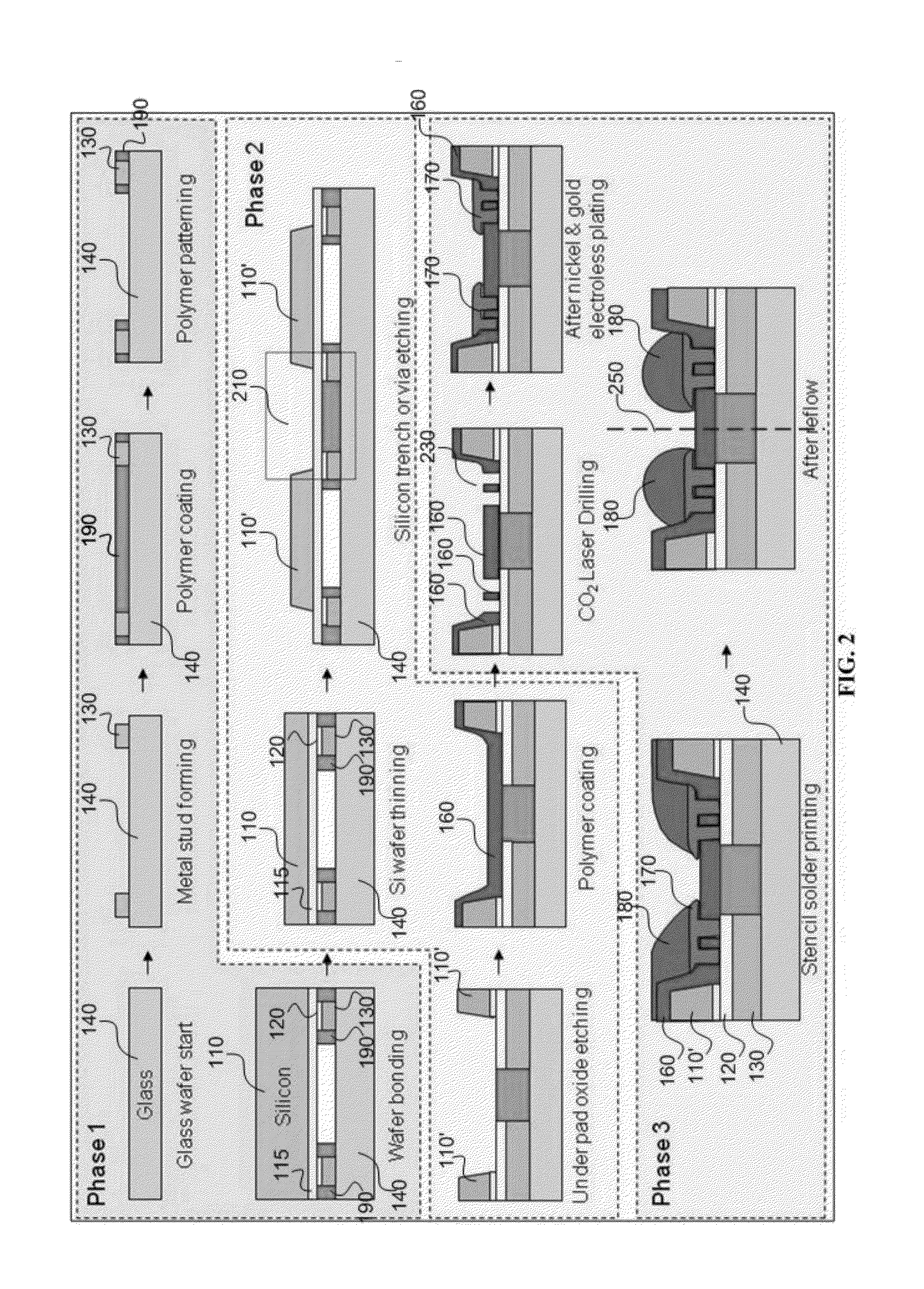
[0017]Turning to the drawings in detail, FIG. 1 depicts a wafer-level device package according to one embodiment of the present invention. Advantageously, packaging of individual devices at the wafer level avoids device contamination by particulates generated during device separation (e.g., dicing). That is, a finished, encapsulated device is formed prior to division into discrete devices such that particulates cannot reach the individual semiconductor chips.

[0018]In the exemplary embodiment of FIG. 1, an image sensor “system on chip”100 is depicted; however, the features described in connection with FIG. 1 are applicable to single layer (that is, not vertically-integrated) device packages as will be discussed below.

[0019]In FIG. 1, an imaging device such as CMOS image sensor 110 has bonding pads 120 positioned thereon. Optionally, metal studs 130 are positioned over the bonding pads 120 to provide additional heat sink capabilities and / or to increase the clearance over image sensor ...


PUM


Abstract

The present invention relates to a semiconductor device packaged at the wafer level such that an entire packaged device is formed prior to separation of individual devices. The semiconductor device package includes a semiconductor chip having one or more bonding pads associated with the chip and a protective layer bonded over the semiconductor chip. An insulation layer is positioned on at least side edges and a lower surface of the semiconductor chip. Interconnection/bump metallization is positioned adjacent one or more side edges of the semiconductor chip and is electrically connected to at least one bonding pad. A compact image sensor package can be formed that is vertically integrated with a digital signal processor and memory chip along with lenses and a protective cover.

Description

COPYRIGHT NOTICE[0001]A portion of the disclosure of this patent document contains material, which is subject to copyright protection. The copyright owner has no objection to the facsimile reproduction by anyone of the patent document or the patent disclosure, as it appears in the Patent and Trademark Office patent file or records, but otherwise reserves all copyright rights whatsoever.FIELD OF THE INVENTION[0002]The present invention relates to wafer-level device packaging and, more particularly, to wafer level device packaging in which device interconnection metallization is positioned adjacent to a functional device.BACKGROUND[0003]Packaging requirements for semiconductor devices have become more stringent as the competing demands of increased functionality and smaller electronic products continue to force device manufacturers to create ever more complex package designs. In particular, increased demands for compact devices have led package manufacturers to pursue vertical integra...

Claims


Application Information

Patent Timeline
Patent Type & Authority Applications(United States)
IPC IPC(8): H01L23/485H01L21/60H01L23/08
CPCH01L27/14632H01L27/14687H01L23/3114H01L2225/06555H01L25/0657H01L25/50H01L2225/06517H01L2225/06589H01L2225/06513H01L2225/06541H01L2224/16157H01L2224/81895H01L2224/215H01L2224/1369H01L2224/13565H01L2224/211H01L2224/2101H01L2224/214H01L2224/16106H01L2224/1183H01L2224/16168H01L24/03H01L24/05H01L24/11H01L24/13H01L24/16H01L24/17H01L24/19H01L24/20H01L24/32H01L24/81H01L24/92H01L24/94H01L24/97H01L2224/03464H01L2224/0401H01L2224/04105H01L2224/05155H01L2224/05644H01L2224/10156H01L2224/1132H01L2224/11849H01L2224/12105H01L2224/131H01L2224/13147H01L2224/1319H01L2224/16148H01L2224/16227H01L2224/16238H01L2224/17181H01L2224/32225H01L2224/73203H01L2224/81191H01L2224/81192H01L2224/81193H01L2224/81447H01L2224/81801H01L2224/9202H01L2224/94H01L2224/97H01L2924/10156H01L2224/92224H01L2224/8185H01L2224/1182H01L2224/92222H01L2224/16225H01L2924/12042H01L2224/16108H01L27/14618H01L2924/00012H01L2924/014H01L2924/0665H01L2924/00014H01L2224/81H01L2224/03H01L2224/11H01L2224/19H01L21/78H01L2924/00
Inventor TSUI, YAT KITYANG, DANLAW, PUI CHUNG
Owner HONG KONG APPLIED SCI & TECH RES INST
Why Eureka
Try Eureka