Semiconductor light device and manufacturing method for the same

Active Publication Date: 2014-01-30
FURUKAWA ELECTRIC CO LTD
View PDF2 Cites 5 Cited by
  • Summary
  • Abstract
  • Description
  • Claims
  • Application Information

AI Technical Summary

Benefits of technology

[0010]Therefore, it is an object of an aspect of the innovations herein to provide a semiconductor light device and a manufacturing method thereof, which are capable of overcoming the above drawbacks accompanying the related art. The above and other objects can be achieved by combinations described in the claims. According to a first aspect of the present invention, provided is a semiconductor light device comprising a semiconductor substrate having a first conduction type; a first cladding layer having the first conduction type deposited above the

Problems solved by technology

However, with the conventional IFVD technique, it is difficult to keep the degree of disordering in the non-window portion low while maintaining a hi

Method used


Image

  • Semiconductor light device and manufacturing method for the same
  • Semiconductor light device and manufacturing method for the same
  • Semiconductor light device and manufacturing method for the same

Examples


first embodiment

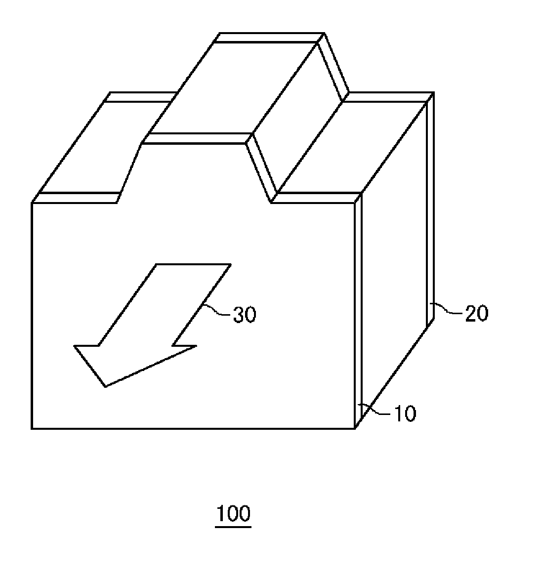
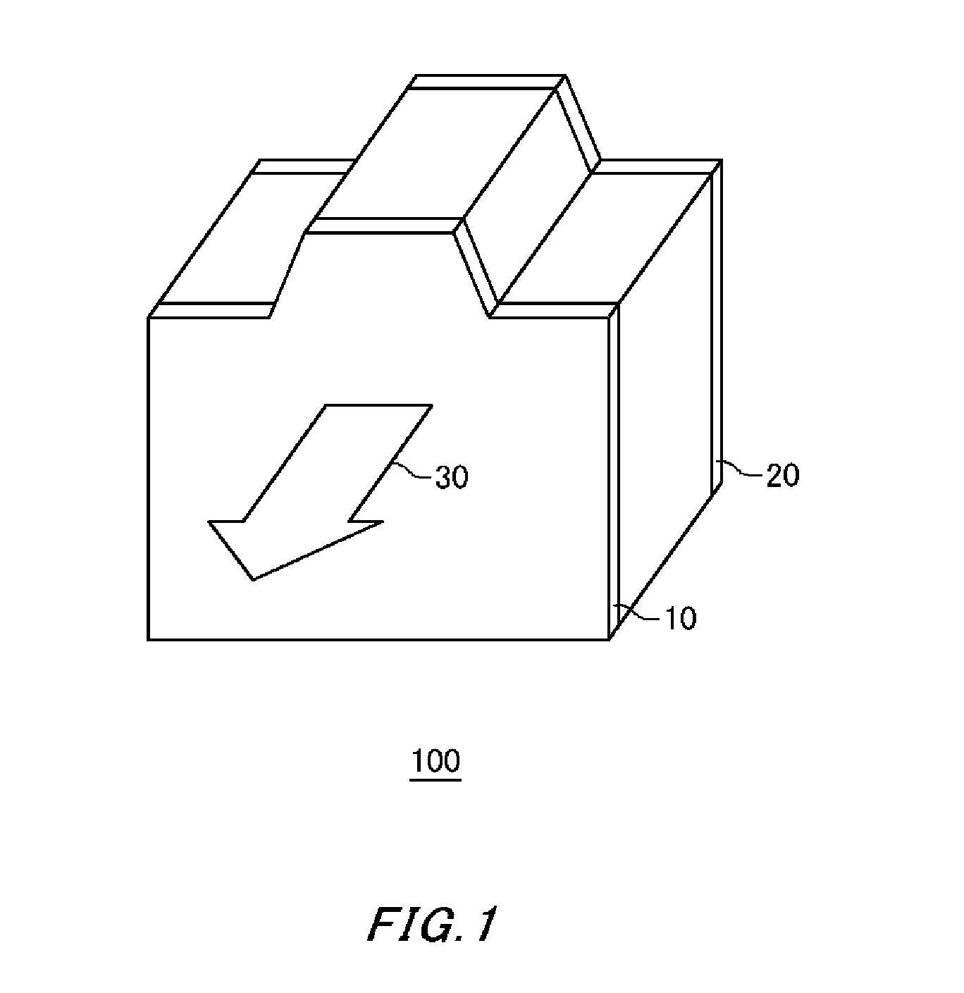
[0044]FIG. 1 is a perspective view of a semiconductor laser element 100 according the present invention. The present embodiment describes an example in which the semiconductor light device is a semiconductor laser element, but the present invention is not limited to this embodiment. The semiconductor laser element 100 may be a Fabry-Perot resonant cavity laser having a ridge structure that confines the current in a striped pattern in the resonant cavity direction. The semiconductor laser element 100 includes a low reflection coating 10 and a high reflection coating 20 at the end surfaces formed by cleaving a wafer. The high reflection coating 20 amplifies the laser light within the resonant cavity by reflecting the laser light. The low reflection coating 10 has a reflectivity with respect to the laser light that is less than that of the high reflection coating 20, and causes laser light that is resonated in the resonant cavity to be output to the outside as the emitted light 30.

[004...

second embodiment

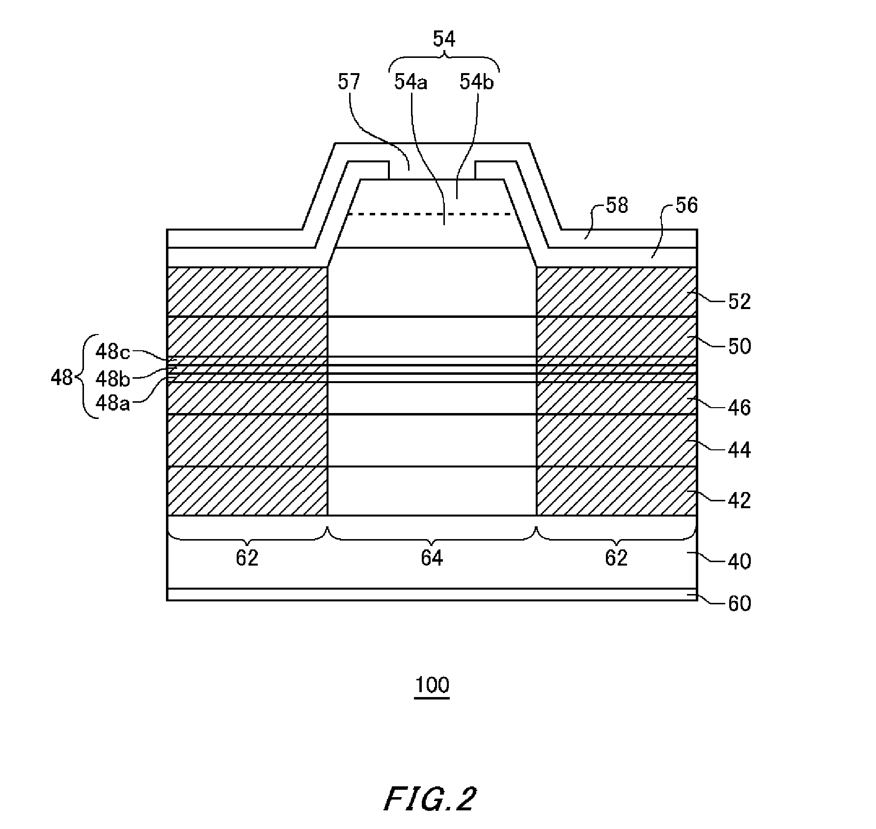
[0085]FIGS. 11 to 15 show steps describing the manufacturing method of the semiconductor laser element 200 according to the present invention. In the same manner as the semiconductor device manufacturing method described above, the semiconductor laser element 200 manufacturing method includes a step of forming a semiconductor layer, a step of depositing two types of dielectric films (first film 70 and second film 72) with different densities on different regions of the semiconductor layer, and a step of forming a window portion 62 and a non-window portion 64 on the semiconductor layer via an annealing process. The step of forming the semiconductor layer includes a step of preparing a semiconductor substrate 40, a step of sequentially depositing, on the semiconductor substrate 40, a plurality of semiconductor layers including the n-type buffer layer 42, the n-type first cladding layer 44, the n-type first guide layer 46, the active layer 48, the p-type second guide layer 50, and the ...

third embodiment

[0094]FIG. 17 is a planar view of an optical waveguide 300 manufactured according to the manufacturing method of the present invention. FIG. 18 is a cross-sectional view over the line A-A of FIG. 17. The optical waveguide 300 includes a semiconductor substrate 310, and a semiconductor layer having a lower cladding layer 320, an optical waveguide layer 330, and an upper cladding layer 340 formed sequentially on the semiconductor substrate 310. The semiconductor layer of the optical waveguide 300 includes a first disordered region 312 that is selectively disordered in a direction perpendicular to the surface of the semiconductor substrate 310, and a second disordered region 314 that is formed to be sandwiched by the first disordered region 312.

[0095]The disordering of the second disordered region 314 is less than the disordering of the first disordered region 312. The disordering of the first disordered region 312 may be at least five times the disordering of the second disordered reg...


PUM


Abstract

Provided is a semiconductor light device comprising a semiconductor substrate having a first conduction type; a first cladding layer having the first conduction type deposited above the semiconductor substrate; an active layer; a second cladding layer having a second conduction type; and a contact layer. The active layer includes a window portion that is disordered via diffusion of vacancies and a non-window portion having less disordering than the window portion, and the contact layer includes a first region and a second region that is below the first region and has greater affinity for hydrogen than the first region.

Description

[0001]The contents of the following patent applications are incorporated herein by reference:[0002]No. 2011-083556 filed in Japan on Apr. 5, 2011,[0003]No. 2011-083867 filed in Japan on Apr. 5, 2011, and[0004]No. PCT / JP2012 / 001876 filed on Mar. 16, 2012.BACKGROUND[0005]1. Technical Field[0006]The present invention relates to a semiconductor light device and a manufacturing method thereof.[0007]2. Related Art[0008]In a semiconductor laser element, in order to prevent damage known as COD (Catastrophic Optical Damage) in the end surfaces through which light is input and output, a technique referred to as IFVD (Impurity-Free Vacancy Disordering) is known as a method for forming a window portion with little laser light absorption by increasing the bandgap energy through disordering of the light input and output surfaces, as shown in Patent Document 1, for example.Patent Document 1: Japanese Patent Application Publication No. 2007-242718[0009]However, with the conventional IFVD technique,...

Claims


Application Information

Patent Timeline
IPC IPC(8): H01L33/30H01L33/00
CPCH01L33/005H01L33/305H01S5/0421B82Y20/00H01S5/028H01S5/2004H01S5/2068H01S5/2072H01S5/22H01S5/3054H01S5/3063H01S5/343H01S5/34313H01S2304/04
Inventor TANIGUCHI, HIDEHIROOHKI, YUTAKA
Owner FURUKAWA ELECTRIC CO LTD
Why Eureka
Try Eureka