Adjustable slot antenna for control of uniformity in a surface wave plasma source

a surface wave plasma and uniformity control technology, applied in the field of semiconductor processing technology, can solve the problems of weak chemical bonding molecules effectively cracking the gas ring, the density of plasma is often substantially non-uniform near the substrate, and the practicability of swp sources still suffers from several deficiencies

Active Publication Date: 2014-01-30
TOKYO ELECTRON LTD
View PDF5 Cites 224 Cited by
  • Summary
  • Abstract
  • Description
  • Claims
  • Application Information

AI Technical Summary

Benefits of technology

[0010]The method includes controlling a plasma property by changing an orientation of a slotted gate plate with respect to the slot antenna. The slotted gate plate is parallel with the slot antenna and is configured to be movable relative to the slot antenna between variable opacity positions. The variable opacity positions include a first opaque position in which at least one first gate slot is misaligned with a fir

Problems solved by technology

However, the practical implementation of SWP sources still suffers from several deficiencies including, for example, plasma stability and uniformity.
For a number of reasons, including charged ions and electrons recombining on chamber walls as they propagate from the source to the substrate, plasma density is often substantially non-un

Method used


Image

  • Adjustable slot antenna for control of uniformity in a surface wave plasma source
  • Adjustable slot antenna for control of uniformity in a surface wave plasma source
  • Adjustable slot antenna for control of uniformity in a surface wave plasma source

Examples


Embodiment Construction

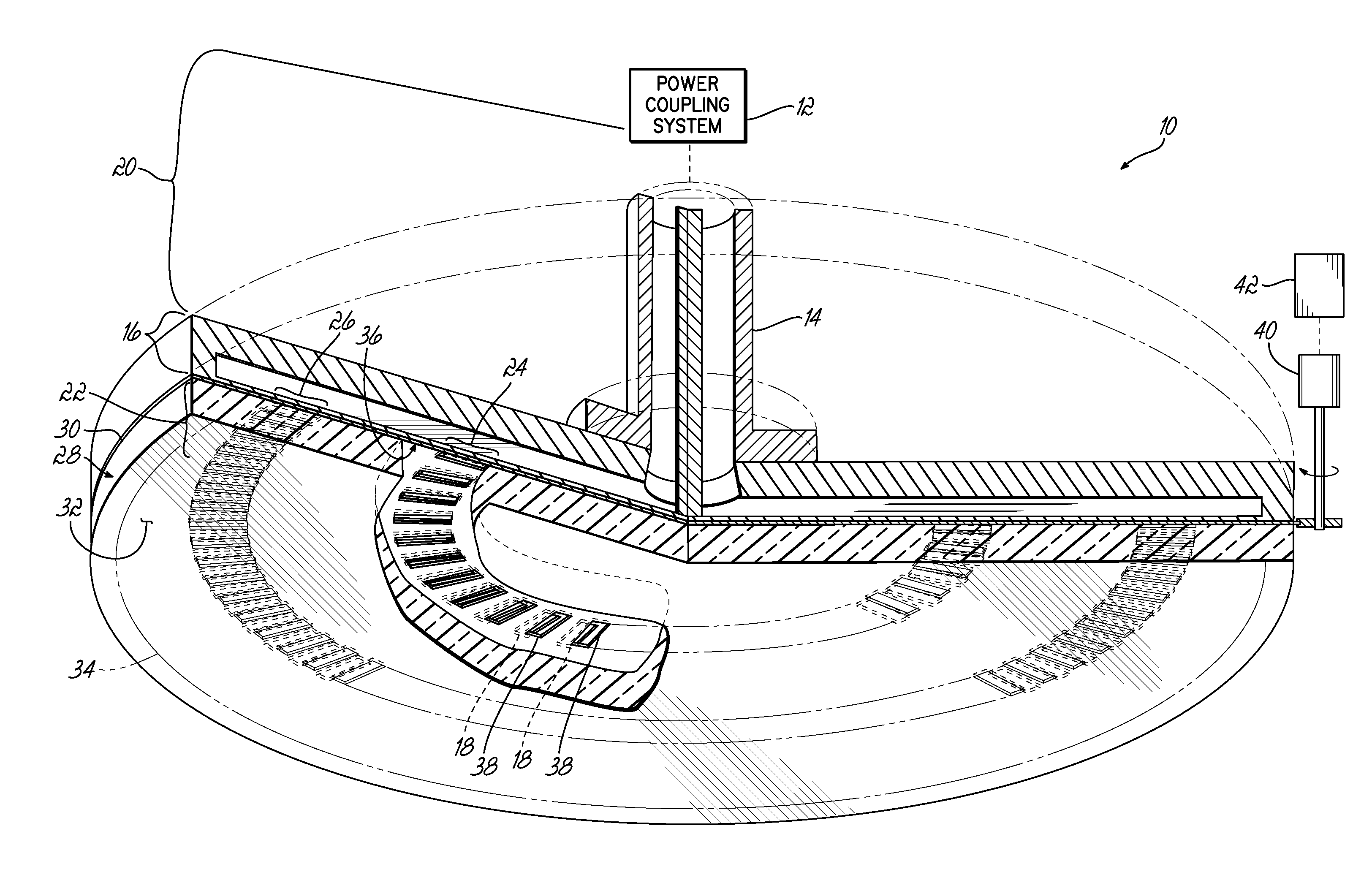
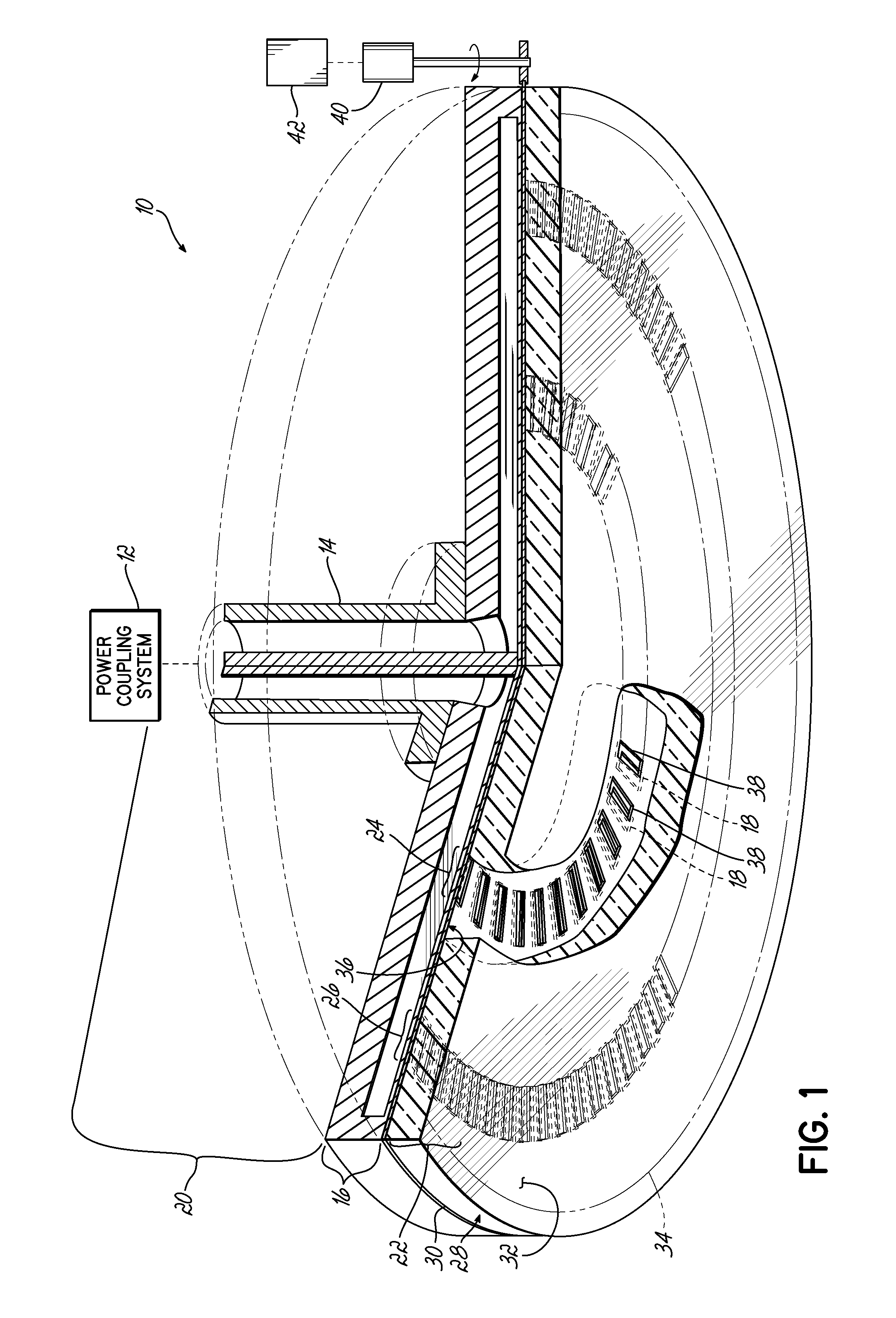
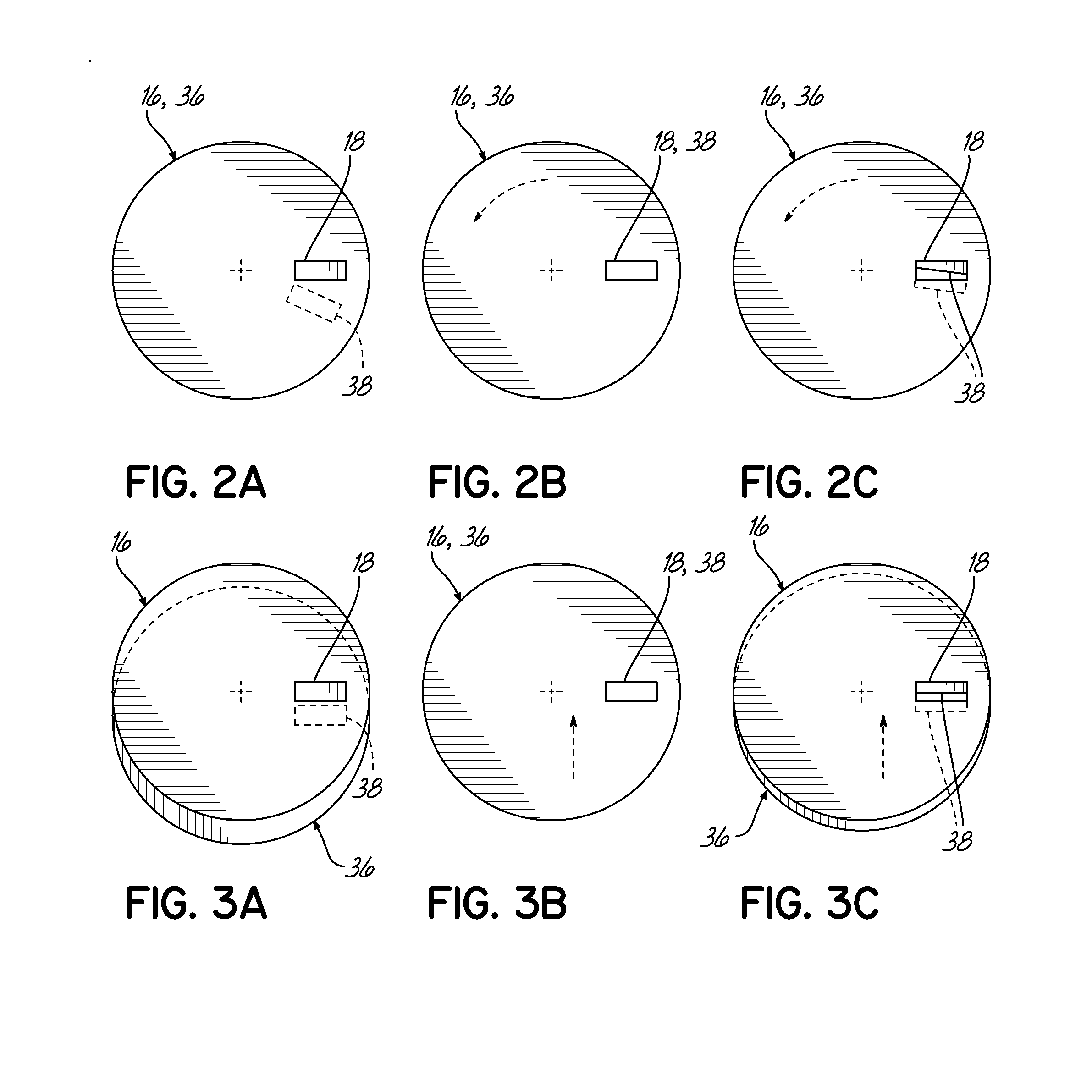
[0017]For more efficient control over plasma properties in a processing chamber, such as radial distribution of the plasma density, radical density distribution, and the electron energy distribution function, the present invention adjusts the microwave power emission from at least one arrangement of antenna slots in a slot antenna assembly of a Surface Wave Plasma Source (“SWPS”). This can be achieved by “turning on” and “turning off” selected antenna slots by occluding at least some portion of the antenna slot aperture by means of a metal disk (“gate”). In the description that follows, even though references may be made to microwaves or other enumerated bands of electromagnetic emissions, it should be understood that the system and method apply to a wide variety of desired electromagnetic wave modes (waves of a chosen frequency, amplitude, and phase).

[0018]FIG. 1 depicts a cross-sectional view of a SWPS 10. A power coupling system 12 provides input EM energy into a wave guide 14, w...


PUM


Abstract

The present invention provides a surface wave plasma source including an electromagnetic (EM) wave launcher comprising a slot antenna having a plurality of antenna slots configured to couple the EM energy from a first region above the slot antenna to a second region below the slot antenna, and a power coupling system is coupled to the EM wave launcher. A dielectric window is positioned in the second region and has a lower surface including the plasma surface. A slotted gate plate is arranged parallel with the slot antenna and is configured to be movable relative to the slot antenna between variable opacity positions including a first opaque position to prevent the EM energy from passing through the first arrangements of antenna slots, and a first transparent position to allow a full intensity of the EM energy to pass through the first arrangement of antenna slots.

Description

CROSS REFERENCE TO RELATED APPLICATION[0001]Pursuant to 37 C.F.R. § 1.78(a)(4), this application claims the benefit of and priority to prior filed co-pending Provisional Application Ser. No. 61 / 674,947, filed Jul. 24, 2012, which is expressly incorporated herein by reference.FIELD OF THE INVENTION[0002]This invention relates to semiconductor processing technology. Specifically, the invention relates to apparatus and methods for controlling properties of a surface wave plasma source.BACKGROUND OF THE INVENTION[0003]Typically, during semiconductor processing, a (dry) plasma etch process is used to remove or etch material along fine lines or within vias or contacts patterned on a semiconductor substrate. The plasma etch process generally involves positioning a semiconductor substrate with an overlying patterned, protective layer, for example a photoresist layer, into a processing chamber.[0004]Once the substrate is positioned within the chamber, it is etched by introducing an ionizable...

Claims


Application Information

Patent Timeline
IPC IPC(8): H05H1/46
CPCH05H1/46H05H1/4615H05H1/463
Inventor VORONIN, SERGEY A.RANJAN, ALOK
Owner TOKYO ELECTRON LTD
Why Eureka
Try Eureka