
Multi-layer water-splitting devices
a multi-layer, water-splitting technology, applied in the manufacture of final products, electrolytic capacitors, electrolysis components, etc., can solve the problems of high cost, high cost, and inability to integrate a transparent polymer substrate, and achieve the effect of low cos
- Summary
- Abstract
- Description
- Claims
- Application Information
AI Technical Summary
Benefits of technology
Problems solved by technology
Method used
Image

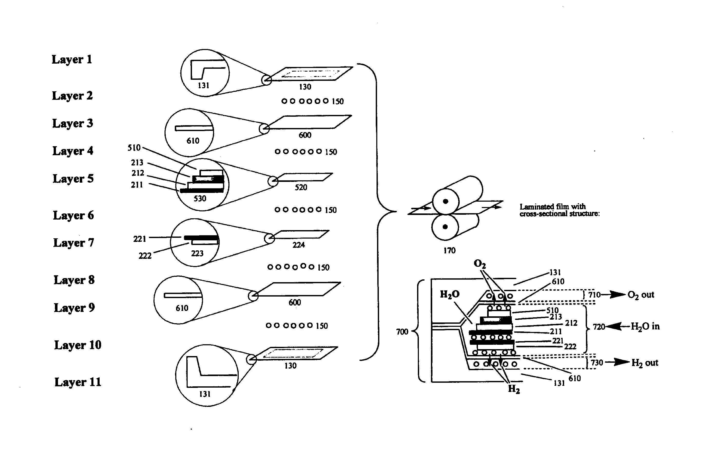
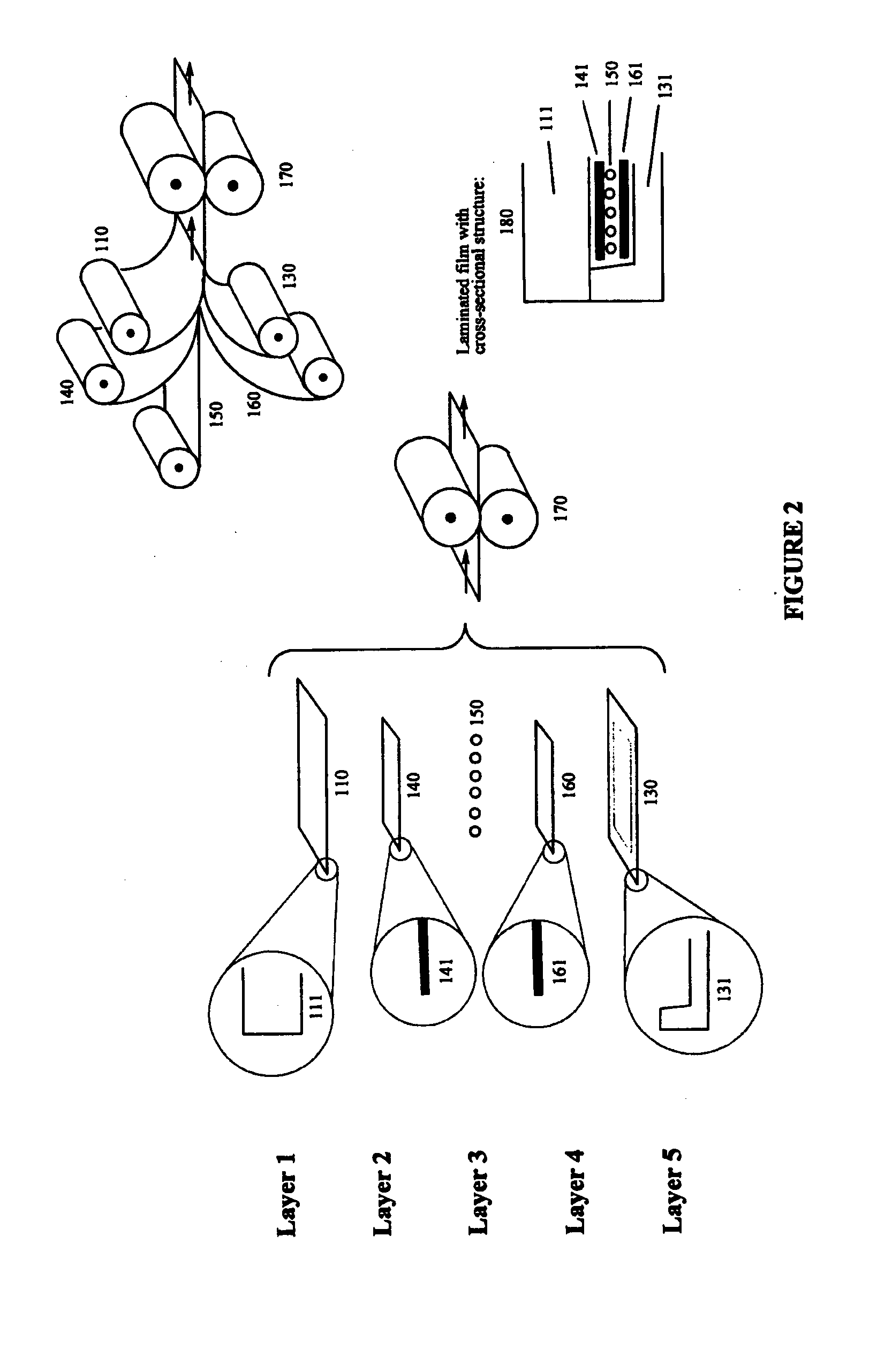
Examples
example 1
General Method for Implementation
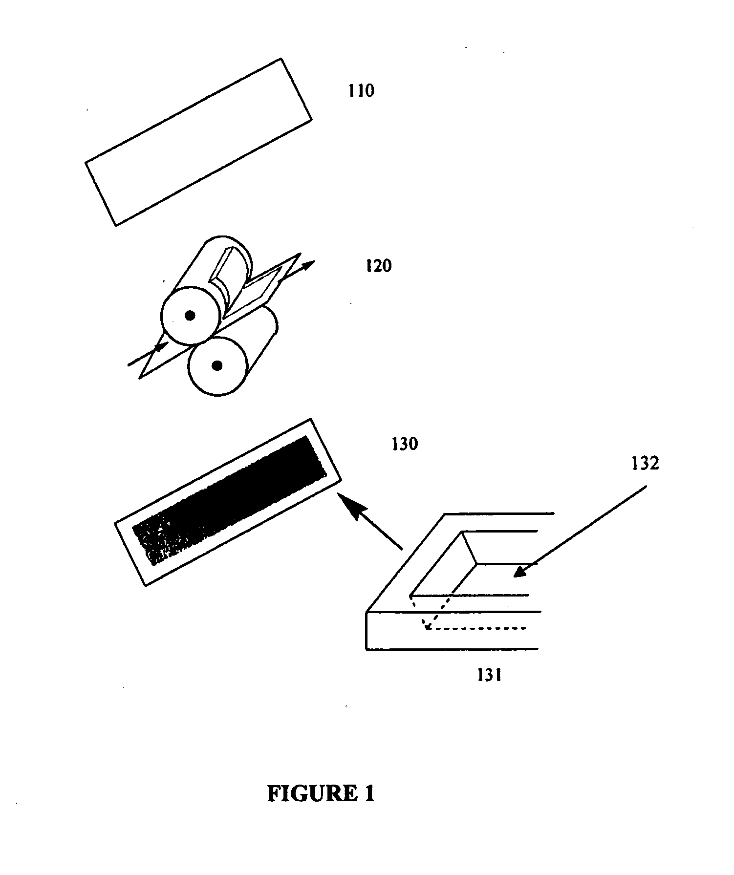
[0072]FIG. 1 illustrates a general method by which suitable recesses may be embossed or impressed into polymer films. As shown in 120, a polymer film 110 is passed between embossing rollers which contain suitable surface relief structures or protrusions, to thereby impart, under high pressure and possibly, heat, at least one recess 132, indentation, depression, cavity or the like, on the embossed or impressed polymer film 130. If desired for particular applications, a plurality of recesses can be provided in polymer film 130. It should be noted that the particular geometric shape or profile of the recess can be varied, the particular profile of recess 132 as illustrated is by way of example only.
[0073]Features can be provided within or integrated as part of the recess, for example being formed during the embossing or impressing process. Such features might include pillars, wells, further recesses, walls, protrusions and / or projections, etc. The featu...
example 2
Fabrication of an Electrochromic Device
[0092]This example describes an improved method of fabrication of an electrochromic device, for example of the type described in International Publication No. WO2007002989 entitled “Charge Conducting Medium” which is incorporated herein by cross-reference.
[0093]FIG. 3 describes a method for manufacturing an electrochromic device. A PVDF membrane 1911 is coated on either side with a conducting layer, such as Ag, Pt, or ITO. The upper conducting layer 1913 is the working electrode and the lower conducting layer 1914 is the counter electrode. The upper conducting layer 1913 (working electrode) is then over-printed on the top side with a conducting polymer layer 1912, which may be PPy, PEDOT, or PANI. The lower conducting layer 1914 (counter-electrode) is overprinted with a different conducting polymer 1915, such as for example, PEDOT. The resulting sub-assembly is designated 190 in FIG. 3. Sub-assembly 190 is co-assembled with a transparent polyme...
example 3
Fabrication of a Back-Contact Dye-Sensitized Solar Cell
[0098]The top sequence in FIG. 4 depicts a method of pre-treating the working electrode in a back-contact dye-sensitized solar cell. The lower schematic in FIG. 4 depicts a process of assembling a back-contact dye-sensitized solar cell.
[0099]Referring to the top sequence in FIG. 4:
[0100]A thin, porous titanium foil 140, having cross-section 211 is dip-coated or printed with a TiO2 layer as shown in step 214. The TiO2 on the coated foil is then sintered by heating at step 215. After sintering, the foil has the cross sectional profile 211, coated with a TiO2 layer 212. The foil is then rolled up at step 216, with spacers placed between the successive layers, to thereby yield the rolled up but separated foil 217. This separated foil 217 is placed in a bath 218 containing a solution of a suitable dye such as ruthenium(II) tris(2,2′-bipyridyl) perchlorate and allowed to soak at step 219. After soaking for a period of time, for exampl...
PUM
| Property | Measurement | Unit |
|---|---|---|
| Volume | aaaaa | aaaaa |
| Flexibility | aaaaa | aaaaa |
| Electrical conductor | aaaaa | aaaaa |
Abstract
Description
Claims
Application Information