Organic light-emitting device

a light-emitting device and organic technology, applied in the direction of thermoelectric devices, solid-state devices, organic chemistry, etc., can solve the problems of unsuitable large-screen displays and damage to the organic layer underlying the ito cathode, and achieve the effect of improving electron injection characteristics and electron mobility

Active Publication Date: 2014-03-13
SAMSUNG DISPLAY CO LTD +1
View PDF4 Cites 55 Cited by
  • Summary
  • Abstract
  • Description
  • Claims
  • Application Information

AI Technical Summary

Benefits of technology

[0009]One or more embodiments of the present invention provides an inverted organic light-emitting device and a normal organic light-emitting device each having an electron transport layer with improved electron injection characteristics and electron mobility.

Problems solved by technology

Polycrystalline silicon is advantageous in view of its high charge mobility and being available for both n-type TFTs and p-type TFTs, but is unsuitable for large-screen displays.
However, the organic layer underlying the ITO cathode may be damaged during deposition of ITO thereon by sputtering.

Method used


Image

  • Organic light-emitting device
  • Organic light-emitting device
  • Organic light-emitting device

Examples


example 1

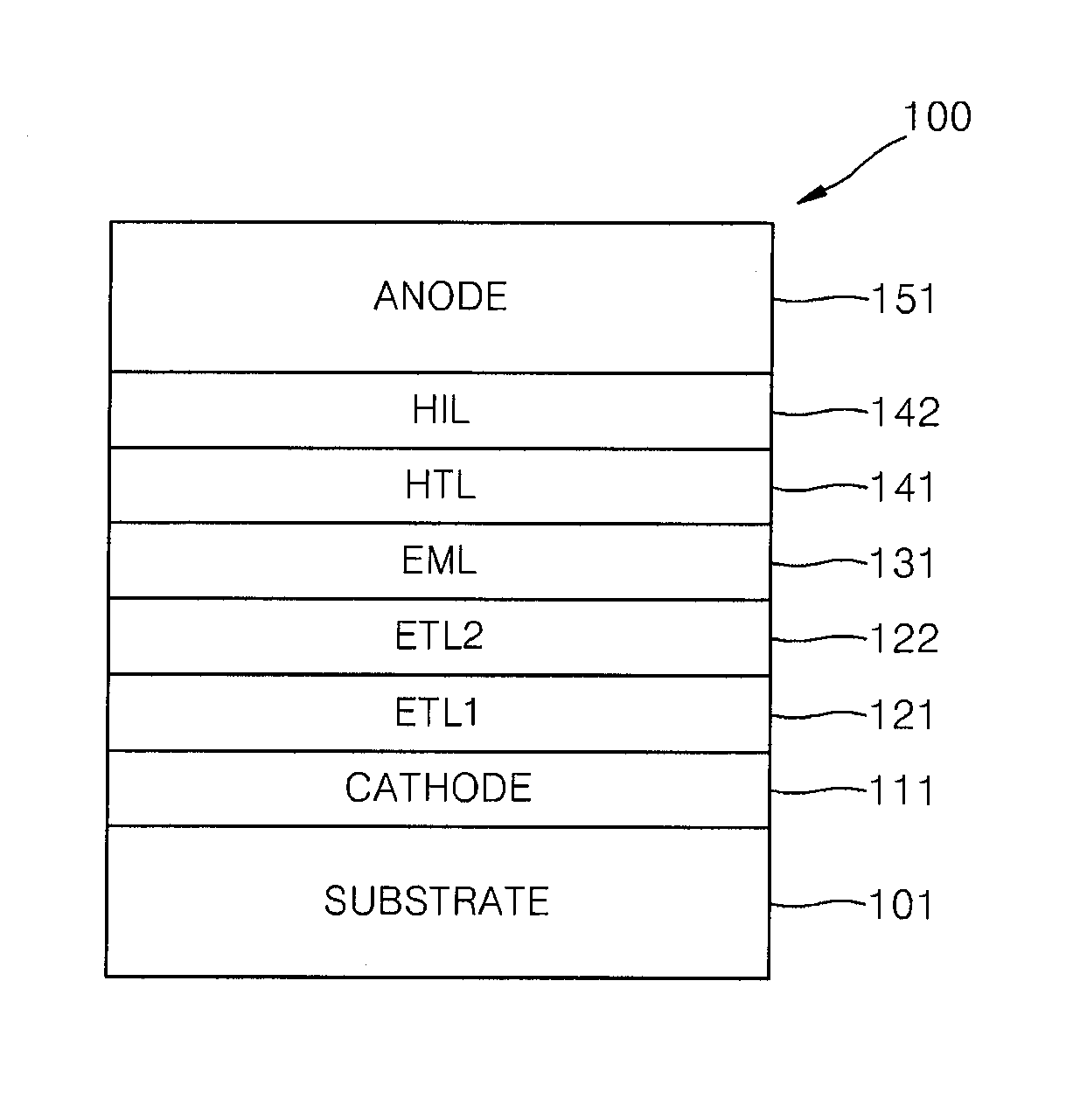
[0084]An ITO-coated glass substrate was cut to a size of 50 mm×50 mm×0.7 mm, and then ultrasonically cleaned with alcohol and then pure water, each for 5 minutes, to prepare the cathode layer on the glass substrate.

[0085]A solution of 0.5 wt % of Merck Green (SPG-01T, Merck Advanced Technologies Limited) and 0.005 wt % of N-DMBI (1 wt % with respect to the weight of Merck Green) dissolved in toluene was prepared. This solution was spin-coated on the ITO glass substrate to form a first electron transport layer containing a mixture of Merck Green: N-DMBI (about 1 wt %) to have a thickness of about 30 nm.

[0086]A TPBi layer having a thickness of about 30 nm was formed by thermal deposition on the first electron transport layer containing Merck Green and N-DMBI to form a second electron transport layer.

[0087]CBP containing 8 wt % of Ir(ppy)3 was vacuum-deposited on the TPBi layer to form an emission layer including an Ir(ppy)3:CBP layer having a thickness of about 10 nm. Afterward, a hol...

example 2

[0090]An OLED was manufactured in the same manner as in Example 1, except that 3 wt % of N-DMBI, instead of 1 wt % of N-DMBI, was used in forming the first electron transport layer.

example 3

[0091]An OLED was manufactured in the same manner as in Example 1, except that 5 wt % of N-DMBI, instead of 1 wt % of N-DMBI, was used in forming the first electron transport layer.


PUM


Abstract

An organic light-emitting device including: a substrate; a transparent cathode on the substrate; an anode disposed opposite to the cathode; an emission layer between the cathode and the anode; and a first electron transport layer between the cathode and the emission layer and including an imidazole derivative.

Description

CROSS-REFERENCE TO RELATED APPLICATION[0001]This application claims priority to and the benefit of Korean Patent Application No. 10-2012-0099544, filed on Sep. 7, 2012, in the Korean Intellectual Property Office, the entire content of which is incorporated herein by reference.BACKGROUND[0002]1. Field[0003]One or more embodiments of the present invention relate to an organic light-emitting device, for example, an organic light-emitting device having an electron transport layer including an n-dopant.[0004]2. Description of the Related Art[0005]Organic light-emitting devices are self-light emitting devices that emit light when a voltage is applied thereto, and offer high luminance, high contrast, multi-color reproduction, large viewing angle, quick response rate, and low driving voltage.[0006]An organic light-emitting device has a structure including an organic emission layer between an anode and a cathode. Upon application of a voltage, holes from the anode and electrons from the cath...

Claims


Application Information

Patent Timeline
Patent Type & Authority Applications(United States)
IPC IPC(8): H01L51/50
CPCH01L51/508H01L51/5076H10K85/342H10K50/166H10K50/165H10K2102/103C07D235/04H01L31/022475H10K50/15H10K50/16
Inventor LEE, SUN-HEESONG, WON-JUNLEE, KWAN-HEELEE, TAE-WOOPARK, MIN-HO
Owner SAMSUNG DISPLAY CO LTD
Why Eureka
Try Eureka